半導体用ガラス 2026-2036年:用途、新技術、市場インサイトGlass in Semiconductors 2026-2036: Applications, Emerging Technologies, and Market Insights 半導体のガラス技術ベンチマーク&分析、サプライチェーンの深堀、キャリア、パネル、IC基板、インターポーザ、IPD、RF-MEMS、フォトニックガラスの各分野における市場予測、課題、機会、採用の見通し &nb... もっと見る

サマリー
半導体のガラス技術ベンチマーク&分析、サプライチェーンの深堀、キャリア、パネル、IC基板、インターポーザ、IPD、RF-MEMS、フォトニックガラスの各分野における市場予測、課題、機会、採用の見通し
半導体のガラスは月並みなコンセプトではなく、すでに近代的なファブの中にひっそりと存在している。超平坦なホウケイ酸ガラスキャリアは、シリコンウェーハの裏面薄片化の際に保持され、ナトリウムフリーのシートはMEMSの気密キャップを形成し、低熱膨張率(CTE)ガラスは多くのウェーハレベルのファンアウトプロセスのベースプレートとなっています。
ガラスは、コア基板、チップをつなぐインターポーザー、サブTHz信号を形成する誘電体、光ファイバーに向かう光子を誘導する誘電体など、背景となる消耗品からパッケージの心臓部へと徐々に移行している。
サイレント・キャリアから高度なパッケージングへ
そのきっかけとなったのは、AIや高性能コンピューティング・デバイスの帯域幅と電力密度の増大である。1台のトレーニング・アクセラレーターには、すでに数千の高速I/Oバンプと、ノイズを最小限に抑えながら数百アンペアを処理する電力供給ネットワークが必要とされている。過去20年間の主力製品であった有機ベースのラミネートは、需要が増え続ける中で、要求される平坦性とビア密度を維持するのに苦労している。シリコンインターポーザーは、はるかに微細な配線を提供するが、価格とパネルサイズが限られた用途にしか対応できない。
ガラスはこの両極端の間をうまくスライドしている。その熱膨張係数はシリコンに合わせて調整することができ、損失正接は40GHzでシリコンより1桁低い。LCD産業からの大型パネル加工の可能性は、歩留まりの上昇に伴ってハイエンドの有機物に向かう傾向のあるコストで、1枚のシートが一辺半メートルになることを意味する。AIと高性能コンピューティングに対する需要の急増により、パッケージング・スタックの各層は、有機ラミネートや第一世代のシリコンインターポーザでさえ快適にサポートできるよりも多くの電流、多くのI/O、より高速の信号伝達を余儀なくされている。このような圧力は、ガラスコア基板と大型パネルガラスインターポーザーを、ニッチな好奇心から商業化へと向かわせました。大手デバイスメーカーや材料ベンダーは現在、この技術を公然と研究している:インテルはアリゾナのパスファインディング・ラインでガラスベースのテスト車両のデモを行い、サムスン電子はI-CubeやH-Cubeパッケージと並ぶ可能性のあるオプションとしてガラスコアを検討し、基板大手のSKCは500mmガラスパネル用のパイロット・ドリル・アンド・フィル・ラインを設置し、ガラス大手のAGCは初期の評価用に低CTEホウケイ酸シートを供給している。AI/HPC時代の次世代基板候補にガラスがしっかりと挙がっているのだ。この傾向は、特に高度なパッケージングやIC基板向けのガラスコア基板やインターポーザーの出現によって反映されている。
高周波とフォトニック集積が対応可能な市場を拡大
ガラスの低誘電損失と光学的透明性は、コンピュート・パッケージングにとどまらない第2の成長エンジンとなっている。Kaバンド以上では、ガラス・マイクロストリップの挿入損失は同等の有機線路の約半分です。
フォトニクスは、さらにもう一つの牽引力となっている。コ・パッケージド・オプティクス(CPO)は、ファイバー・アタッチメントをスイッチのフロントパネルから、スイッチASICから数ミリメートル離れた基板に移すことを目指している。設計されたガラスは、電気再配分層と低損失導波路の両方を運ぶことができ、アライメントを簡素化し、高価なシリコンフォトニックインターポーザを排除することができます。RFに使用されるのと同じガラス貫通ビア(TGV)技術で垂直光ビアを形成できるため、1つのコアでトランスインピーダンスアンプ、レーザードライバー、光導波路そのものをサポートできる。このようなエレクトロニクスとフォトニックの融合は、ガラスの強みを直接生かし、従来のエレクトロニクス・パッケージングの枠を超えて、その潜在的な市場を押し広げます。
 なぜ今サプライチェーンの洞察が重要なのか
ガラスがパイロットラインから量産体制に入るには、原料の入手可能性よりも、レーザー穴あけ、銅フィリング、 パネルハンドリング、設計の自動化といった新しいエコシステムに左右されます。歩留まりの学習曲線、ビアフィルの信頼性、パネルの反り、デザインキットの成熟度によって、ガラスがシス テムインテグレーターの設定したコスト目標を達成できるかどうかが決まります。したがって、誰が生産能力を導入しているのか、どの穴あけ技術が概念実証から24時間365日の生産体制に移行しているのか、設計ツールがギガヘルツ帯の損失やサブミクロンの反りをどれだけ早くモデル化できるのかを理解することは、採用のタイミングに賭ける者にとって不可欠である。
同様に重要なのは、シリコンや改良有機物との競争力である。ファウンドリは、ガラスが持つフィーチャーサイズの優位性を狭めるハイブリッドウェーハレベルの再配分を推進し、ラミネートサプライヤーは、より低い粗さと優れたCTEマッチングを持つ次世代ABFコアを開発しています。本レポートでは、これらの材料の長所と短所をベンチマークしているため、読者はガラスが勝者となる可能性が高い分野と、特殊な選択肢に留まる分野を明確に把握することができます。
本レポートの特徴
本レポートは、キャリアウェーハからフォトニックタイルまで、7つの物理的製品クラス別にセグメント化した初のボトムアップ市場モデルを提供しています。本レポートでは、1年ごとの単位需要と収益を定量化し、発表されたパネル生産能力と予測出荷量を対応させ、ガラス貫通穴あけ、メタライゼーション、多層膜再配分における技術準備状況を分析している。また、ガラスの電気的・機械的優位性の背後にある物理学的な説明、残された加工上の課題の概説、高周波RFとフォトニクスの統合がアドレス可能な総市場に与える影響の評価も行っています。読者は、2036年までに44億米ドルのビジネスチャンスがあるという明確なイメージを得ることができます。
半導体デバイス設計者はチップレットロードマップを計画し、パッケージングエンジニアは次の基板技術を選択し、材料サプライヤーはパネルスケールのガラスラインを検討し、装置ベンダーはレーザードリルや平坦化ツールを開発し、投資家は先端パッケージングの次の変遷を探す。本レポートは、材料科学、プロセス技術、市場経済、最終用途の需要を一つの物語にまとめ、関係者が十分な情報を得た上で技術的・戦略的な意思決定を行うために必要な状況を提供する。
主な内容
目次1.要約
1.1. ガラス材料
1.2. ガラスの半導体への応用
1.3. 先端パッケージング用ガラス
1.4. さまざまな半導体用途に使用されるガラス
1.5. ガラスパッケージングの先にある機会
1.6. ガラス基板の主な利点
1.7. ガラス基板採用の課題
1.8. 今後の市場動向
1.9. 今後の開発方向性:高度な処理技術
1.10.今後の開発方向性:統合パッケージングソリューションと持続可能な製造イニシアチブ
1.11.ガラスコア基板導入の受益者
1.12. ガラス基板のバリューチェーン
1.13. 有機基板からガラスコア基板へのバリューチェーンの移行
1.14.今後の展望
1.15. 素材イノベーション
1.16. 投資重点分野
1.17. 代表的プレイヤーの活動
2. 市場予測
2.1. 市場予測セグメンテーション
2.2. 市場予測手法
2.3. 2025~2036年の市場金額予測
2.4. 2025~2036年の市場価値予測
2.5. 市場動向
2.6. 2025年対2036年市場
2.7. 市場および経済要因
3. 先端パッケージングおよびIC基板におけるガラス
3.1. 先端パッケージングの次元性
3.2. 1D半導体パッケージングから
3.3. 先端パッケージング 2Dおよび2D+
3.4. 先端パッケージング 2.5Dおよび3D
3.5. 先端パッケージング 3.5Dおよび4D
3.6. 2.5Dおよび3Dパッケージングの技術開発動向
3.7. インテルの先進的なパッケージングロードマップ
3.8. 異種統合ソリューション
3.9. システムオンチップ(SOC)の概要
3.10. マルチチップモジュール(MCM)の概要
3.11. システムインパッケージ(SiP)
3.12. システムインパッケージ(SiP)の分析
3.13. 有機コア基板からガラスコア基板へ
3.14. ガラスIC基板
3.15. 半導体におけるパッケージング基板の進化
3.16. 有機コアからガラスコアへ
3.17. 有機コア基板とガラスコア基板の比較
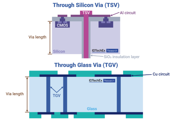
3.18. TSV vs. TGV
3.19. 先端パッケージングのための材料特性比較
3.20. ガラスの機械的および信頼性に関する主な利点
3.21. I/O 密度
3.22. ガラス基板上の微細回路パターンを可能にする主な要因
3.23. 微細回路パターンは自由度を減少させる
3.24.FC-BGA 基板はより大きな歪みをもたらす
3.25. ビア形成の限界
3.26. SAP法の限界
3.27. PCB スタックアップ
3.28. 従来の多層 PCB とビルドアップ PCB の比較
3.29. ビルドアップ材料:ABF
3.30. ABF基板の製造プロセス3.24. FC-BGA基板はより大きな歪みをもたらす
3.31. FC-BGA(Flip Chip Ball Grid Array)基板
3.32. ガラスコア基板
3.33. ガラスコア基板技術
3.34. ガラスインターポーザ vs. シリコンインターポーザ
3.35. ガラス貫通ビア形成
3.36.ガラスビア形成プロセス
3.37.ガラス貫通ビア形成プロセスの比較
3.38. TGVプロセスとビア形成方法
3.39. 機械的および高出力レーザー穴あけ
3.40. レーザー誘起ディープエッチング
3.41. BSPからのLMCE
3.42. Philoptics 社の TGV 技術
3.43. レーザー誘起修飾と高度なウェットエッチング
3.44. TGV プロセス間の比較
3.45. 感光性ガラスとウェットエッチング
3.46. Samtec 社の TGV 技術
3.47. 高アスペクト比の TGV
3.48. TGVメタライゼーション
3.49.TGVメタライゼーションプロセス
3.50. 2段階プロセス
3.51. TGVメタライゼーションにおけるシード層成膜
3.52. TGVメタライゼーション代替プロセスの 要因
3.53. TGVメタライゼーションプロセスの比較
3.54. ガラス基板の製造
3.55. 技術:有機コア基板 vs. ガラスコア基板
3.56. ガラスコア基板:コア層の製造
3.57. ガラスコア基板:ビルドアップ層の製造
3.58. ガラス基板の製造プロセス (CHIMES)
3.59. ガラス基板上で2/2μm L/Sを実現
3.60. ジョージア工科大学によるガラス製造プロセス
3.61. ガラスコアの3次元集積化: ジョージア工科大学によるガラスキャビティ積層プロセスフロー
3.63. チップファーストの非TSV 3Dガラスパネル埋め込み
3.64. ジョージア工科大学のテスト車両比較
3.65. インテルのガラスライン
3.66. ガラスベースの先進パッケージングおよびIC基板の特徴
3.67. TGV - 主要企業と製品のベンチマーク
3.68. ガラスパッケージの先進的な熱管理
3.69. ガラスコア基板およびインターポーザーの特許活動における動向の変化と新興リーダー
3.70. 半導体パッケージングにおけるガラス基板採用の革新
3.71. ガラスの革新への取り組み
3.72. Plan Optik AG
3.73. Plan Optik AGの技術
3.74. KCC
3.75. インテルのガラス基板への取り組み
3.76. Absolicsの進展
3.77. CHIMESの先端パッケージングにおけるガラスへの注目
4. フォトニクスにおけるガラス
4.1. フォトニック集積回路とは
4.2. なぜPICなのか
4.3. 光結合 - I/O
4.4. EIC/PIC集積
4.5. Co-Packaged Optics
4.6. Co-Packaged Opticsアーキテクチャ
4.7. 光トランシーバの主要トレンド
4.8. ガラスベースのCPO集積
4.9. ガラスインターポーザベースのCPOアーキテクチャ
4.10. イオン交換導波路形成技術
4.11. デュアルモードガラス導波路の性能特性
4.12.CPO統合のための断熱ガラス-シリコン導波路結合
4.13. CPOアプリケーション向けガラスベース光ファイバコネクタアセンブリ
4.14. ガラスインターポーザーの光信号経路アーキテクチャ
4.15. ガラスインターポーザーの製造プロセスとレーザー分離技術
4.16. コーニングの高密度102.4Tb/sガラス統合プラットフォーム
4.17. ガラスインターポーザーによるEIC/PICの3D統合
4.18. EIC、PIC、ASICをガラス基板上に3D統合
4.19. ASIC、EIC、PICを同一パッケージ基板上に3D統合する製造プロセス
4.20. フォトニクス用ガラス集積の進歩
5. 高周波アプリケーションにおけるガラス
5.1. 半導体・電子機器パッケージにおける低損失材料の応用
5.2. 高周波PCB設計における伝送損失
5.3.低損失材料としてのガラス
5.4. 半導体技術においてガラスが可能にするRFアプリケーションのカテゴリー
5.5. LTCCとガラス材料のベンチマーク
5.6. 誘電率:異なる無機基板(LTCC、ガラス)の安定性対周波数
5.7. 5G PCB/部品用市販低損失材料のベンチマーク
5.8. 低損失材料の選択に影響を与える5つの重要な指標
5.9. ガラスサプライヤー: JSKの低透過損失積層板用HF-F
5.10. ガラスサプライヤー:SCHOTTのFLEXINITY connect
5.11. ガラスサプライヤー:AGC/ALCAN Systemの窓用透明アンテナ
5.12. フィルター基板としてのガラス
5.13. アドバンスト・セミコンダクター・エンジニアリング社のの5G向けガラス集積受動素子(IPD)フィルター
5.14. 5G用ガラス基板AiP:ジョージア工科大学
5.15. 6G用ガラス:ジョージア工科大学
5.16. 6G用ガラスインターポーザ
BSPからのLMCE

Summary
Glass in semiconductors technology benchmarks & analysis, supply-chain deep dive, market forecasts across carrier, panel, IC-substrate, interposer, IPD, RF-MEMS & photonic glass segments, challenges, opportunities and adoption outlook
Glass in semiconductors is not a moon-shot concept; it already sits quietly inside modern fab. Ultra-flat borosilicate carriers hold silicon wafers during backside thinning, sodium-free sheets form hermetic MEMS caps, and low-coefficient of thermal expansion (CTE) glass is the baseplate for many wafer-level fan-out processes.
Glass is gradually moving from a background consumable to the heart of a package, providing the core substrate, the interposer that links chiplets, and the dielectric that shapes sub-THz signals or steers photons on their way to optical fiber.
From silent carrier to advanced packaging
The catalyst is the escalating bandwidth and power density of AI and high-performance-computing devices. A single training accelerator already requires thousands of high-speed I/O bumps and a power-delivery network that handles hundreds of amps with minimal noise. Organic-based laminate, the workhorse of the last twenty years, struggles to keep the required flatness and via density with ever increasing demand. Silicon interposers offer far finer wiring, but at a price and panel size that limited applications can justify.
Glass slides neatly between these extremes. Its coefficient of thermal expansion can be tailored to match silicon; its loss tangent is an order of magnitude lower than silicon at 40 GHz, and large-panel processing potential from the LCD industry means a single sheet can be half a meter on one side at costs that trend towards high-end organics as yields rise. The surging demand for AI and high-performance computing is forcing every layer of the packaging stack to carry more current, more I/O, and higher signaling speeds than organic laminates or even first-generation silicon interposers can comfortably support. These pressures have turned glass core substrates and large-panel glass interposers from a niche curiosity into commercialization. Leading device makers and materials vendors are now openly investigating the technology: Intel has demonstrated glass-based test vehicles on its Arizona path-finding line, Samsung Electronics is exploring glass cores as a potential option alongside its I-Cube and H-Cube packages, substrate major SKC has installed a pilot drill-and-fill line for 500 mm glass panels, and glass giant AGC is supplying low-CTE borosilicate sheets for early evaluations. No company has yet nailed down a production launch date, but the collective effort signals a clear shift—glass is firmly on the shortlist of next-generation substrate candidates for the AI/HPC era. The trend is reflected by the emergence of glass core substrate and interposers, especially for advanced packaging and IC substrates.
High-frequency and photonic integration widen the addressable market
Glass's low dielectric loss and optical transparency give it a second growth engine beyond compute packaging. At Ka-band and above, insertion loss through a glass microstrip is roughly half that of an equivalent organic line.
Photonics adds still another pull. Co-packaged optics (CPO) aims to move fiber attach from the front panel of a switch to the substrate that sits millimeters from the switch ASIC. Engineered glass can carry both the electrical redistribution layers and the low-loss waveguides, simplifying alignment and eliminating costly silicon photonic interposers. Because the same through-glass via (TGV) technology used for RF can create vertical optical vias, a single core can support trans-impedance amplifiers, laser drivers, and the optical waveguide itself. This convergence of electronic and photonic routing plays directly to glass's strengths and pushes its potential market beyond conventional electronics packaging.
Why supply-chain insight matters now
Glass's march from pilot lines to volume hinges less on raw material availability—melting furnaces exist in every region—than on the emerging ecosystem of laser drilling, copper filling, panel handling and design automation. Yield learning curves, via-fill reliability, panel warpage and design-kit maturity will determine whether glass meets the cost targets set by system integrators. Understanding who is installing capacity, which drilling techniques are moving from proof-of-concept to 24/7 production, and how quickly design tools can model gigahertz losses or sub-micron warpage is therefore essential for anyone betting on the timing of adoption.
Equally important is the competitive dynamic with silicon and improved organics. Foundries are pushing hybrid wafer-level redistribution that narrows the feature-size advantage glass holds, while laminate suppliers are developing next-generation ABF cores with lower roughness and better CTE matching. This report benchmarks pros and cons across these materials so readers can see clearly where glass is likely to win—and where it will remain a specialty option.
What this report delivers
This report provides the first bottom-up market model segmented by seven physical product classes, from carrier wafers through to photonic tiles. It quantifies unit demand and revenue year by year, maps announced panel capacity against forecast shipments, and analyses technology readiness in through-glass via drilling, metallization, and multilayer redistribution. The study also explains the physics behind glass's electrical and mechanical advantages, outlines the processing challenges that remain, and evaluates the impact of high-frequency RF and photonic integration on total addressable market. Readers will gain a clear picture of how large the opportunity is—US$4.4 billion by 2036.
Who should read
Semiconductor device architects planning chiplet roadmaps, packaging engineers choosing their next substrate technology, materials suppliers eyeing panel-scale glass lines, equipment vendors developing laser drilling or planarization tools, and investors looking for the next inflection in advanced packaging will all find insights here. The report connects material science, process technology, market economics and end-application demand into a single narrative, giving stakeholders the context they need to make informed technical and strategic decisions.
Key Aspects
Table of Contents1. EXECUTIVE SUMMARY
1.1. Glass materials
1.2. Applications of glass in semiconductors
1.3. Glass for advanced packaging
1.4. Glass used in various semiconductor applications
1.5. Opportunities ahead with glass packaging
1.6. Key advantages of glass substrates
1.7. Challenges in adopting glass substrates
1.8. Future market trends
1.9. Future development directions: Advanced processing technologies
1.10. Future development directions: Integrated packaging solutions & Sustainable manufacturing initiatives
1.11. Beneficiaries of glass core substrate introduction
1.12. Value chain of glass substrate
1.13. Value chain shift from organic to glass core substrate
1.14. Future outlook
1.15. Material innovations
1.16. Investment priority areas
1.17. Activities of representative players
2. MARKET FORECAST
2.1. Market forecast segmentation
2.2. Market forecast methodology
2.3. Unit shipment forecast 2025-2036
2.4. Market value forecast 2025-2036
2.5. Market trends
2.6. 2025 vs. 2036 markets
2.7. Market and economic factors
3. GLASS IN ADVANCED PACKAGING AND IC SUBSTRATE
3.1. Dimensionality of advanced packaging
3.2. From 1D semiconductor packaging
3.3. Advanced packaging 2D & 2D+
3.4. Advanced packaging 2.5D & 3D
3.5. Advanced packaging 3.5D & 4D
3.6. Technology development trend for 2.5D and 3D packaging
3.7. Intel's advanced packaging roadmap
3.8. Heterogeneous integration solutions
3.9. Overview of System on Chip (SOC)
3.10. Overview of Multi-Chip Module (MCM)
3.11. System in Package (SiP)
3.12. Analysis of System in Package (SiP)
3.13. Glass IC substrates
3.14. From Organic to Glass Core Substrate
3.15. Evolution of packaging substrates in semiconductors
3.16. From organic to glass core
3.17. Organic core substrate vs. glass core substrate
3.18. TSV vs. TGV
3.19. Material property comparison for advanced packaging
3.20. Key mechanical and reliability benefits of glass
3.21. I/O density
3.22. Key factors enabling fine circuit patterns on glass substrates
3.23. Fine circuit patterning reduces DoF
3.24. FC-BGA substrates lead to larger distortions
3.25. Limitations of Via formation
3.26. SAP method limitations
3.27. PCB stack-ups
3.28. Traditional multilayer vs. build-up PCBs
3.29. Build-up material: ABF
3.30. ABF substrate manufacturing process
3.31. Flip Chip Ball Grid Array (FC-BGA) substrate
3.32. Glass core substrate
3.33. Glass core substrate technologies
3.34. Glass interposer vs. silicon interposer
3.35. Through Glass Via Formation
3.36. Through glass via formation process
3.37. Comparison of through glass via formation processes
3.38. TGV process and via formation methods
3.39. Mechanical and high-power laser drilling
3.40. Laser-induced deep etching
3.41. LMCE from BSP
3.42. Philoptics' TGV technology
3.43. Laser-induced modification and advanced wet etching
3.44. Comparison among the TGV processes
3.45. Photosensitive glass and wet etching
3.46. Samtec's TGV technology
3.47. TGV of high aspect ratio
3.48. TGV Metallization
3.49. TGV metallization processes
3.50. Two-step process
3.51. Seed layer deposition in TGV metallization
3.52. Factors for alternative TGV metallization process
3.53. Comparison of TGV metallization processes
3.54. Glass Substrate Manufacturing
3.55. Technology: Organic core substrate vs. glass core substrate
3.56. Glass core substrate: Core layer fabrication
3.57. Glass core substrate: Build-up layer fabrication
3.58. Manufacturing process of glass substrate (CHIMES)
3.59. Achieving 2/2 μm L/S on glass substrate
3.60. Glass fabrication process by Georgia Institute of Technology
3.61. Glass core 3D integration: Georgia Tech's embedded die packaging
3.62. Glass cavity lamination process flow by Georgia Institute of Technology
3.63. Chip-first non-TSV 3D glass panel embedding
3.64. Georgia Institute of Technology test vehicle comparison
3.65. Intel's glass line
3.66. Features of Glass-based Advanced Packaging and IC Substrates
3.67. TGV - Player and products benchmark
3.68. Advanced thermal management for glass packages
3.69. Shifting dynamics and emerging leaders in glass core substrate and interposer patent activity
3.70. Glass substrate adoption innovations in semiconductor packaging
3.71. Glass innovation efforts
3.72. Plan Optik AG
3.73. Plan Optik AG's Technology
3.74. KCC
3.75. Intel's glass substrate efforts
3.76. Absolics' progresses
3.77. CHIMES' focus on glass in advanced packaging
4. GLASS IN PHOTONICS
4.1. What is a photonic integrated circuit?
4.2. Why PICs?
4.3. Optical coupling - I/O
4.4. EIC/PIC integration
4.5. Co-Packaged Optics
4.6. Co-packaged optics architecture
4.7. Key trend of optical transceiver
4.8. Glass-based CPO integration
4.9. Glass interposer-based CPO architecture
4.10. Ion exchange waveguide formation technology
4.11. Dual-mode glass waveguide performance characteristics
4.12. Adiabatic glass-to-silicon waveguide coupling for CPO integration
4.13. Glass-based fiber connector assembly for CPO applications
4.14. Glass interposer optical signal path architecture
4.15. Glass interposer manufacturing process and laser separation technology
4.16. Corning's high-density 102.4 Tb/s glass integration platform
4.17. 3D integration of EIC/PIC with a glass interposer
4.18. 3D integration of EIC, PIC, ASIC on a co-packaged glass substrate
4.19. Fabrication process of the 3D integration of ASIC, EIC, PIC on a co-packaged substrate
4.20. Advancements in glass integration for photonics
5. GLASS IN HIGH-FREQUENCY APPLICATIONS
5.1. Applications of low-loss materials in semiconductor and electronics packaging
5.2. Transmission loss in high-frequency PCB design
5.3. Glass as a low-loss material
5.4. Categories of RF applications enabled by glass in semiconductor technology
5.5. Benchmark of LTCC and glass materials
5.6. Dielectric constant: Stability vs frequency for different inorganic substrates (LTCC, glass)
5.7. Benchmarking of commercial low-loss materials for 5G PCBs/components
5.8. Five important metrics impacting low-loss materials selection
5.9. Glass suppliers: JSK's HF-F for low transmission loss laminates
5.10. Glass suppliers: SCHOTT's FLEXINITY connect
5.11. Glass suppliers: AGC/ALCAN System's transparent antennas for windows
5.12. Glass as a filter substrate
5.13. Glass integrated passive devices (IPD) filter for 5G by Advanced Semiconductor Engineering
5.14. Glass substrate AiP for 5G: Georgia Tech
5.15. Glass for 6G: Georgia Tech
5.16. Glass interposers for 6G
5.17. Access More With an IDTechEx Subscription
ご注文は、お電話またはWEBから承ります。お見積もりの作成もお気軽にご相談ください。本レポートと同分野(ケミカル)の最新刊レポート
IDTechEx社の 半導体、コンピュータ、AI - Semiconductors, Computing & AI分野 での最新刊レポート
よくあるご質問IDTechEx社はどのような調査会社ですか?IDTechExはセンサ技術や3D印刷、電気自動車などの先端技術・材料市場を対象に広範かつ詳細な調査を行っています。データリソースはIDTechExの調査レポートおよび委託調査(個別調査)を取り扱う日... もっと見る 調査レポートの納品までの日数はどの程度ですか?在庫のあるものは速納となりますが、平均的には 3-4日と見て下さい。
注文の手続きはどのようになっていますか?1)お客様からの御問い合わせをいただきます。
お支払方法の方法はどのようになっていますか?納品と同時にデータリソース社よりお客様へ請求書(必要に応じて納品書も)を発送いたします。
データリソース社はどのような会社ですか?当社は、世界各国の主要調査会社・レポート出版社と提携し、世界各国の市場調査レポートや技術動向レポートなどを日本国内の企業・公官庁及び教育研究機関に提供しております。
|
|