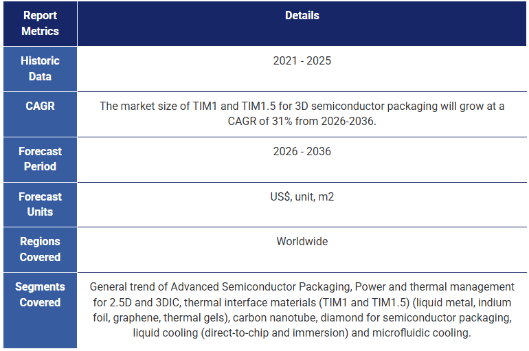
2026年から2036年までの先進半導体パッケージングにおける熱管理:技術、市場、および機会Thermal Management for Advanced Semiconductor Packaging 2026-2036: Technologies, Markets, and Opportunities 10年間のTIM1/TIM1.5予測(グラフェン、液体金属、熱伝導ゲル、インジウム箔別)およびマイクロ流体冷却の10年間予測。ASP(先進半導体パッケージング)における熱管理と電力管理の詳細な分析。 ... もっと見る

サマリー
10年間のTIM1/TIM1.5予測(グラフェン、液体金属、熱伝導ゲル、インジウム箔別)およびマイクロ流体冷却の10年間予測。ASP(先進半導体パッケージング)における熱管理と電力管理の詳細な分析。
AI計算需要と高性能チップの熱設計電力(TDP)が継続的に増加し、業界が2.5Dから3Dパッケージングアーキテクチャへの移行を進める中、熱管理は大規模な商業化と採用の主要な障壁として浮上しています。この課題に対応するため、業界は先進的な熱材料(液体金属、ダイヤモンド、グラフェンなど)、チップの蓋なし設計、電力供給ネットワークの最適化、背面電力供給の実現、液体およびマイクロ流体冷却技術の採用など、多様な戦略を模索しています。
IDTechExのレポート「Thermal Management for Advanced Semiconductor Packaging 2026-2036: Technologies, Markets, and Opportunities」は、2.5Dから3D先進半導体パッケージング(ASP)への移行、電力供給方法の進展(例:背面電力供給やシリコン貫通ビア)、 3D集積回路パッケージングに伴う熱的課題、革新的な熱材料(熱界面材料やダイヤモンド基板など)の活用、および液体冷却技術(ダイレクト・トゥ・チップ、浸漬、マイクロ流体冷却システムなど)の採用について、包括的な分析を提供しています。
レポートの主要な内容は以下の通りです:
2.5Dおよび3D半導体パッケージングにおける熱管理の課題
2025年現在、TSMCのCoWoS技術など、2.5D半導体パッケージングはB200のような高性能チップにおける主要なアプローチとして依然として主流です。パフォーマンスをさらに向上させるため、特に帯域幅と遅延の面で、業界は3Dパッケージングへの移行に注力する傾向が強まっています。2.5Dアーキテクチャでは、ロジックダイと垂直に積層された高帯域幅メモリ(HBM)が共有インターポーザ上に並列に配置されるのに対し、3Dパッケージングではアクティブダイを別のアクティブダイの上に直接積層します。この垂直統合は性能向上の可能性を秘めていますが、電力と熱管理の課題が大幅に増加する要因となります。
3D ICにおける電力供給の課題
3D ICでは、電流密度の上昇、ピンアクセスの制限、垂直インターコネクトの使用により、電力供給が2Dに比べて大幅に複雑化します。k層の3Dスタックは、同じ面積の2Dチップに比べて約k倍の電流を消費しますが、電力ピンやパッケージングリソースはそれに応じてスケールしません。この不均衡が複数の課題を引き起こします。電源供給に用いられるTSVは、スタックあたり約1 Ωの大きな抵抗を導入し、IR降下を増加させ、安定した供給電圧を維持する困難を引き起こします。電源は通常、スタック全体の累積電流を負担する最下層を通じて供給されるため、電圧降下や動的ノイズに特に脆弱です。さらに、電力消費の多い計算ブロックがヒートシンクに近い最下層に配置されるため、状況はさらに複雑化します。一方、TSVと高密度配線によりデカップリングコンデンサを配置するスペースが制限されるため、効果的なデカップリングが妨げられます。これらの複合的な影響はスタック全体の電圧変動を悪化させ、性能の変動性、タイミングの不確実性、信頼性リスクを増加させます。特にピーク負荷条件下ではこの影響が顕著になります。
3D ICにおける熱的課題
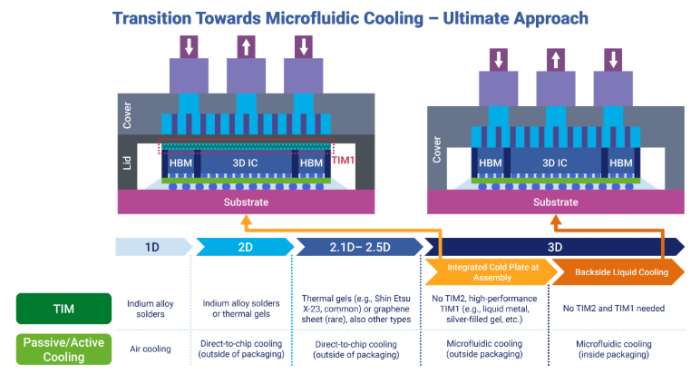
熱管理は、3D ICにおける最も重要なボトルネックの一つです。2D設計では熱が横方向と上方向へヒートシンクに向かって拡散する一方、3Dスタックは薄いダイから構成されており、横方向の熱拡散が制限されます。さらに、中間ダイはヒートシンクから遠く離れており、有効な熱逃避経路が限られているため、熱の蓄積が発生しやすいです。また、ダイ間の絶縁層や接着剤などの低熱伝導率の材料により、垂直方向の熱除去経路が制限されます。これにより、熱スポットが発生し、インターコネクトの漏れや応力増加により性能が低下し、信頼性が低下します。もう一つの重要な課題は、高出力ロジックブロックとメモリの近接配置により、層間の熱結合が著しくなり、熱設計をさらに複雑化させる点です。従来の冷却方法は埋込層に効果的に到達できないため、熱TSVやチップレベルマイクロ流体冷却などの代替技術を検討する必要があります。しかし、これらの方法は設計複雑性、コスト、統合課題といったトレードオフを伴います。
熱伝導効率向上のための材料革新
2.5Dおよび3D半導体パッケージングにおけるより効率的な熱管理を支援するため、業界は複数の革新的なソリューションを積極的に探求しています。その中でも特に注目されている分野は、高度な熱界面材料(TIM)の開発です。IDTechExのレポート「先進半導体パッケージングにおける熱管理 2026-2036:技術、市場、機会」は、TIM技術の詳細な分析を提供しており、特にTIM1と新興のTIM1.5カテゴリーに焦点を当てています。これらの材料には、液体金属、インジウム箔、グラフェンシート、および熱伝導性を向上させた次世代熱ゲルなどが含まれます。
2025年現在、信越化学のX23は、ボールグリッドアレイ(BGA)アプリケーションにおいて広く採用されているTIM1材料です。しかし、先進チップの熱設計電力が上昇する中、業界はより高い性能を提供する新規のTIM1およびTIM1.5材料への移行を加速させています。有望な候補には、液体金属、グラフェンベースの材料、高導電性充填剤を配合した熱伝導ゲルなどが挙げられます。
並行して、伝統的な2層構造のTIM(TIM1とTIM2)から、単一のTIM1.5層への移行が進んでいます。このアプローチは、材料の界面を最小化することで熱抵抗を低減することを目的としています。この変更によりTIM層の数が減少する可能性がありますが、TIM1.5材料は技術仕様の厳格さから単位コストが高くなる傾向にあるため、市場全体が縮小するとは限りません。IDTechExは、TIM1とTIM1.5の合計市場が2036年までに約5億ドルに達すると予測し、大きな商業的機会を強調しています。
TIMを超えて、もう1つの有望な研究分野は、特に銅メッキダイヤモンドを基材材料として使用する高級半導体パッケージングへのダイヤモンドの応用です。IDTechExの報告書では、ダイヤモンド基材を先進的なパッケージングアーキテクチャに統合する最新の開発動向、技術的課題、将来の見通しについても詳しく分析しています。
液体冷却、浸漬冷却、およびマイクロ流体冷却
材料の革新を超えて、アクティブ液体冷却は高度な熱管理における重要なトレンドとしてますます注目されています。高性能データセンターでは、ダイレクト・トゥ・チップや浸漬冷却などの技術が既に商業展開段階に達しています。特に、前年においてNvidiaのGB200およびNVLink72構成で冷板冷却が採用されたことは、その短期的な主要ソリューションとしての地位をさらに固めました。IDTechExは、コールドプレート冷却が少なくとも今後2~3年間は主要なアプローチとして維持されると予測しています。
しかし、コールドプレート冷却と浸漬冷却は主にチップパッケージから周囲環境への熱放散に対応しています。より緊急の熱課題はパッケージ自体にあり、具体的には3Dパッケージングアーキテクチャにおける垂直に積み重ねられたコンポーネント間の熱管理です。現在、業界はこの問題に対する明確な解決策を確立できていません。
IDTechExは、マイクロ流体冷却をこの内部熱的ボトルネックを解決する有望な候補として特定しています。ただし、その実装には複雑さが伴います。マイクロ流体冷却は、パッケージの蓋内またはパッケージ構造の内部に液体冷却剤を循環させるために、複雑なマイクロチャネルのネットワークを利用します。さまざまなアーキテクチャ構成が開発中ですが、この技術は依然として、設計と製造の複雑さ、スケーラビリティに関する懸念、長期的な信頼性に関するデータ不足など、複数の課題に直面しています。
IDTechExの報告書は、マイクロ流体冷却に関する進行中の研究開発活動を詳細に分析し、先進的な半導体パッケージングにおける今後の採用に向けた潜在的なアーキテクチャのロードマップを提示しています。
.png) 結論
3Dパッケージングへの移行により、帯域幅と効率の向上を実現するため、熱課題に対応するための複数のソリューション(例:裏面電源供給、統合型電圧レギュレーター、高度なTIM1、マイクロ流体冷却など)が提案され、調査されてきました。2025年半ば現在、TSV密度、製造複雑さ、欠陥率のトレードオフ、マイクロ流体冷却と商業的スケーラビリティのバランスなど、依然として重大な課題が存在しています。そのため、業界関係者はこれらの課題の解決に注力しており、IDTechExのレポート「Thermal Management for Advanced Semiconductor Packaging 2026-2036: Technologies, Markets, and Opportunities」は、潜在的なパッケージングアーキテクチャの革新、新規材料、アクティブ冷却戦略、および今後10年間における異なる技術の市場成長見通しについて、包括的な概要を提供しています。
主要なポイント
本報告書は、先進的な半導体パッケージング(2.5Dおよび3D)の電力と熱管理に関する課題、新規熱伝導材料、および液体冷却ソリューションの動向に関する重要な市場情報を提供します。
具体的には以下の内容を含みます:
目次1. エグゼクティブサマリー
1.1. 半導体パッケージングの進化ロードマップ
1.2. HPCチップにおける2.5Dおよび3D IC統合の比較表
1.3. HPCチップ向け先進半導体パッケージングにおける電力課題
1.4. HPCチップ向け電力管理コンポーネントの概要
1.5. 2.5D統合におけるPDN性能への主要設計パラメータの影響
1.6. 3DICにおける電力供給の課題
1.7. 3DICにおける熱の課題
1.8. 次世代HPCチップ向けのバックサイド電力供給
1.9. BSPDNにおける重要な熱課題の概要:ホットスポット、冷却、材料
1.10. 先進パッケージングにおけるTSV信頼性のための設計およびプロセス考慮事項
1.11. TSV電気的性能に影響を与える主要なプロセス要因
1.12. 横方向電力供給(LPD)から縦方向電力供給(VPD)への移行
1.13. 明日のCoWoS:機能的インターポーザーへの移行
1.14. TIM1に関する考慮事項
1.15. 今後のTIM1の選択肢
1.16. 基板材料としてのダイヤモンド - 課題
1.17. HPC向けのベンチマーク冷却技術
1.18. マイクロ流体冷却への移行 - 究極のアプローチ
1.19. 高出力2.5D/3Dパッケージ向け冷却戦略の概要 - 1
1.20. 高出力2.5D/3Dパッケージ向け冷却戦略の概要 - 2
1.21. タイプ別のTIM1およびTIM1.5のASP市場シェア予測:2026-2036(面積ベース)
1.22. TIM1およびTIM1.5の面積予測:2026-2036
1.23. TIM1およびTIM1.5の市場規模予測:2026-2036
1.24. タイプ別のTIM1およびTIM1.5のASP市場シェア予測:2026-2036(市場規模ベース)
1.25. マイクロ流体冷却ASPユニット予測:2026-2036
1.26. IDTechExサブスクリプションでさらにアクセス
2. はじめに
2.1. 熱設計電力(TDP)
2.2. HPC(高性能コンピューティング)チップの10年間のTDPトレンド
2.3. HPCチップにおけるTDP増加を促進する主要因
2.4. 半導体パッケージングの進化ロードマップ
2.5. HPCチップにおける2.5D対3D IC先進半導体パッケージング技術
2.6. HPCチップにおける2.5Dおよび3D IC統合の比較表
2.7. 2.5D/3Dパッケージの熱特性と課題
2.8. HPCチップにおける先進半導体パッケージングの熱的利点
2.9. なぜ2.5Dパッケージング技術が今日の高性能HPCチップで支配的なのか
2.10. 先進パッケージングにおけるTDPの影響の概要
2.11. GPUにおける2.5Dおよび3Dパッケージングの実際の事例
2.12. 高出力2.5D/3Dパッケージ向け冷却戦略の概要 - 1
2.13. 高出力2.5D/3Dパッケージ向け冷却戦略の概要 - 2
3. 2.5Dおよび3D先進半導体パッケージング技術の概要と開発ロードマップ
3.1. 半導体パッケージングの進化ロードマップ
3.2. 半導体パッケージング - 技術の概要
3.3. 先進半導体パッケージング性能の主要指標
3.4. 半導体パッケージングにおける相互接続技術の概要
3.5. 2.5Dパッケージング構造の概要
3.6. バンピング技術の進化
3.7. バンプのスケーリングにおける課題
3.8. 先進半導体パッケージングのためのμバンプ
3.9. バンプレスCu-Cuハイブリッドボンディング
4. 2.5Dおよび3DICにおける電力管理
4.1.1. チャプターのイントロダクション
4.2. HPC向け先進半導体パッケージングにおける電力供給の導入
4.2.1. HPCチップの先進半導体パッケージングにおける電力課題
4.2.2. HPCチップ向け電力管理コンポーネントの概要
4.2.3. 先進的な電力供給ネットワーク(PDN)
4.2.4. PDN性能に影響を与える主要な電力供給ノイズ(PSN)指標
4.2.5. 動的電圧および周波数スケーリング(DVFS)
4.2.6. パワーゲーティング
4.2.7. クロックゲーティング
4.2.8. 熱管理ランタイムループ
4.2.9. パッケージ内電圧調整(OPVR)
4.2.10. デカップリングコンデンサ(デキャップ)
4.2.11. 低抵抗インタコネクト
4.3. 2.5Dの電力供給ネットワーク(PDN)評価
4.3.1. 2.5Dインターポーザ統合プラットフォームにおける電力供給ネットワークの評価
4.3.2. 2.5Dブリッジ統合プラットフォームにおける電力供給ネットワークの評価
4.3.3. 2.5DブリッジチップにおけるPDNの統合
4.3.4. ブリッジチップPDNにおけるP/Gネットワーク統合の影響
4.3.5. 2.5Dブリッジへのデカップリングコンデンサの追加
4.3.6. デカップリングの過剰設計とトレードオフ
4.3.7. ブリッジチップサイズおよび静電容量密度のトレードオフの影響
4.3.8. 2.5D統合におけるPDN性能への主要設計パラメータの影響
4.3.9. TSVのPDN性能への影響
4.3.10. バンプピッチがPDN性能に与える影響
4.4. 3Dの電力供給ネットワーク(PDN)評価
4.4.1. 3DICの台頭の概要
4.4.2. 3DICにおける電力供給の課題 - (1)
4.4.3. 3DICにおける電力供給の課題 - (2)
4.4.4. 3DICにおける熱の課題
4.4.5. 先進的な3DIC統合のトレンド
4.4.6. バックサイド電力供給ネットワーク(BSPDN) - 1
4.4.7. バックサイド電力供給ネットワーク(BSPDN) - 2
4.4.8. 3つの主要なBPDアーキテクチャ
4.4.9. 埋め込まれた電力レール(BPR)
4.4.10. BSPDNが熱挙動に与える影響 - imec研究
4.4.11. BSPDNにおける重要な熱課題の概要:ホットスポット、冷却、材料
4.4.12. BSPDN熱最適化戦略
4.4.13. 3DICにおけるBSPDNの利点、課題、熱的影響の概要
4.4.14. Through Si Via(TSV)
4.4.15. TSV製造プロセス
4.4.16. 3DICにおけるTSV
4.4.17. 例:高密度TSVを用いた3D統合のためのウェハーレベルF2B Cu-Cuハイブリッドボンディング
4.4.18. 先進パッケージングにおけるTSV信頼性のための設計およびプロセス考慮事項
4.4.19. TSV電気的性能に影響を与える主要なプロセス要因
4.4.20. TSVのスケーリングトレンド
4.4.21. 3D IC統合におけるTSVの熱モデリングと影響
4.5. 業界プレイヤーからの事例研究
4.5.1. TSMC: CoWoS-Lの主要開発特徴
4.5.2. 次世代AIチップ向けTSMC CoWoS-L
4.5.3. ディープトレンチキャパシタ(DTC) vs 従来型コンデンサ
4.5.4. 3DIC向けディープトレンチキャパシタ(DTC) - 1
4.5.5. 3DIC向けディープトレンチキャパシタ(DTC) - 2
4.5.6. 明日のCoWoS: 機能的インターポーザーへの移行
4.5.7. インターポーザーにおけるIVR統合に関する技術的課題
4.5.8. SPILの先進的な2.5Dソリューション: FOEB-T
4.5.9. SPILのパフォーマンスベンチマーク: FOEB vs FOEB-T vs 2.5D Siインターポーザー
4.5.10. ASE: HPCシステム向けPowerSiP?プラットフォーム
4.5.11. ASE: FOCoS-B(TSVあり/なし)の例と仕様
4.5.12. Samsung: 2.5Dパッケージングソリューション(I-Cube)
4.6. 横方向電力供給(LPD)から縦方向電力供給(VPD)への移行
4.7. 既存の電圧レギュレータ技術
4.8. SRAM-on-Logic 3Dパッケージングにおける熱改善
4.9. 先進的な3Dパッケージングにおける熱挙動とヒートシンクの最適化
4.10. 大型2.5DパッケージングにおけるPCM vs 熱グリースの熱的安定性比較
5. 高度なパッケージングのための新しい熱材料とソリューション
5.1. はじめに
5.1.1. 3Dパッケージングと高度な熱管理の傾向
5.1.2. CPU、GPU、メモリモジュールのダイアタッチ
5.1.3. 3D半導体パッケージングにおけるTIM1の傾向
5.1.4. ダイアタッチ材料の比較
5.1.5. TIM1の使用場所
5.1.6. TIM1の考慮事項
5.1.7. 液体冷却オプション
5.2. 熱インターフェース材料
5.2.1. パッケージ内の熱インターフェース材料 - TIM1
5.2.2. 将来のTIM1の可能なオプション
5.2.3. インジウム箔TIM1 - 複数回の再フロー工程に関する問題
5.2.4. 伝統的かつ成熟した製品 - BGA用の新エツX-23シリーズ
5.2.5. 熱ゲル - 新エツMicroSi
5.2.6. 銀充填熱グリース - FCBGA向けの潜在的解決策
5.2.7. グラフェン - TIM1.5としての使用が証明され、ResonacのグラフェンがTIM1として使用されている
5.2.8. グラフェン - 裸ダイ + TIM1.5、最も人気のある方法はラッピング工程
5.2.9. 液体金属 - 2.5DパッケージングのためのTIM1またはTIM1.5
5.2.10. 液体金属の課題とインジウム社による固体/液体アプローチの解決策
5.2.11. インジウム社 - 液体金属
5.2.12. 雲南中軒液体金属技術有限公司
5.2.13. 雲南中軒 - 液体金属の業界標準確立への支援
5.2.14. サーバー向けの液体金属 - Nvidia 5090
5.2.15. 縦方向に配置されたグラファイトフィラーを使用した熱伝導シートをTIM1として使用
5.2.16. Resonac TIMs
5.2.17. Arieca - 液体金属埋め込みエラストマー(LMEEs)
5.2.18. Arieca - LMEEsのテスト
5.2.19. ホットスポットを避けるためのTIM0としてのダイヤモンド - 初期研究段階
5.2.20. 液体金属およびSiOx TIMを用いた統合型Siマイクロクーラー
5.2.21. チップおよびパッケージレベル - CuNWs/PDMSベースのTIM
5.2.22. 液体CuNW注入ナノ構造複合材料としてのTIM(1/2)
5.2.23. 液体CuNW注入ナノ構造複合材料としてのTIM(2/2)
5.3. ASPにおけるダイヤモンドの使用
5.3.1. Cu/ダイヤモンド基板 - 小規模テスト
5.3.2. ダイヤモンド/Cu基板の課題
5.3.3. 3Dパッケージングのためのダイヤモンドヒートシンク冷却ソリューション
5.3.4. Cu/ダイヤモンド製造 - コールドスプレー
5.3.5. 埋め込まれた金属構造を持つ熱強化マイクロバンプ
5.3.6. 高い熱伝導性を実現するためのCu-Cu間拡散結合
5.3.7. 効率的な熱管理のためのダイヤモンド-チップ-ガラスインターポーザ
5.3.8. ダイヤモンドインターポーザ - 熱放散の調査
5.3.9. ダイヤモンド基板 - 単結晶か多結晶か?
5.3.10. ダイヤモンド基板材料 - 課題
6. 液体冷却
6.1. 概要
6.1.1. 液体冷却と浸漬冷却
6.1.2. 液体冷却技術の比較(1)
6.1.3. 液体冷却技術の比較(2)
6.1.4. 液体冷却 - ラックレベルでの異なる冷却技術の電力制限
6.1.5. チップレベルでの異なる冷却技術
6.1.6. 冷却技術の比較
6.2. チップ直結冷却(D2C)
6.2.1. 液体冷却コールドプレート
6.2.2. コールドプレート冷却の利点と欠点
6.2.3. コールドプレートシステムの熱コスト分析(1)
6.2.4. コールドプレートシステムの熱コスト分析(2)
6.2.5. 単相コールドプレート
6.2.6. 単相コールドプレートの考慮事項
6.2.7. なぜ単相コールドプレートが支配的になる可能性があるのか
6.3. 浸漬冷却
6.3.1. 単相および二相浸漬 - 概要(1)
6.3.2. 単相浸漬冷却(2)
6.3.3. SWOT:単相浸漬冷却
6.3.4. 概要:二相浸漬冷却
6.3.5. SWOT:二相浸漬冷却
6.3.6. 単相浸漬冷却のロードマップ
6.3.7. 二相浸漬冷却のロードマップ
6.4. マイクロ流体冷却
6.4.1. HPCのためのベンチマーク冷却技術
6.4.2. マイクロ流体の概要
6.4.3. HPCパッケージの冷却構成のベンチマーク
6.4.4. マイクロチャネルの性能ベンチマーク研究
6.4.5. マイクロチャネルヒートシンクアーキテクチャの設計原則と課題(1)
6.4.6. マイクロチャネルヒートシンクアーキテクチャの設計原則と課題(2)
6.4.7. 冷却のためのウェーハレベルマイクロチャネル統合
6.4.8. マイクロチャネルシステムの熱設計考慮事項と冷却材の選択
6.4.9. マイクロチャネル統合とシステム導入の障壁
6.4.10. Microsoft - 統合シリコンマイクロ流体冷却
6.4.11. マイクロ流体冷却ヒートシンク構造と製造
6.4.12. HPC向けのオンパッケージ液体冷却
6.4.13. imec - マイクロ流体冷却(1/2)
6.4.14. imec - マイクロ流体冷却(2/2)
6.4.15. インテルファウンドリの熱機能、TIMオプション、パッケージ内液体冷却
6.4.16. IBM z17
7. 予測
7.1. TIMの変数に関する仮定
7.2. GPUの平面ダイパッケージング面積の傾向
7.3. CoWoS - 開発進捗とロードマップ
7.4. TIM1とTIM1.5の市場シェア予測(タイプ別、面積ベース、2026-2036年)
7.5. TIM1とTIM1.5の面積予測(2026-2036年、ASP向け)
7.6. TIM1とTIM1.5の考慮事項
7.7. TIM1とTIM1.5の市場規模予測(2026-2036年、ASP向け)
7.8. TIM1とTIM1.5の市場シェア予測(タイプ別、市場規模ベース、2026-2036年)
7.9. マイクロ流体冷却ASPユニット予測(2026-2036年)
7.10. データセンター向け液体冷却予測(D2Cおよび浸漬冷却、2025-2035年)
8. プロフィール
8.1. Accelsius ? 二相直接チップ冷却
8.2. Amkor ? 高度な半導体パッケージング
8.3. Arieca
8.4. ASE ? 高度な半導体パッケージング
8.5. Asperitas Immersed Computing
8.6. Carbice
8.7. Green Revolution Cooling (GRC)
8.8. LiquidCool Solutions ? シャーシベースの浸漬冷却
8.9. Resonac Holdings Corporation: 液晶アクリルエラストマー(LCE)
8.10. サムスン電子(メモリ)
8.11. 深圳HFC
8.12. Smart High Techと上海瑞喜
8.13. 住友化学株式会社
8.14. TSMC(高度な半導体パッケージング)
8.15. ZutaCore

Summary
Ten-year TIM1/TIM1.5 forecast for advanced semiconductor packaging (ASP) split by graphene, liquid metal, thermal gel, and indium foil. 10-year forecast for microfluidic cooling. Detailed analysis on thermal and power management for ASP.
As AI computing demands and the thermal design power (TDP) of high-performance chips continue to rise, and the industry shifts from 2.5D to 3D packaging architectures, thermal management has emerged as a key barrier to large-scale commercialization and adoption. To address this growing challenge, the industry is exploring a range of strategies, including the use of advanced thermal materials (such as liquid metal, diamond, and graphene), lidless chip designs, optimization of the power delivery network, implementation of backside power delivery, and the adoption of liquid and microfluidic cooling technologies.
The IDTechEx report, "Thermal Management for Advanced Semiconductor Packaging 2026-2036: Technologies, Markets, and Opportunities", provides a comprehensive analysis of the transition from 2.5D to 3D advanced semiconductor packaging (ASP), advancements in power delivery methods (e.g., backside power and through-silicon vias), thermal challenges associated with 3D integrated circuit packaging, the use of innovative thermal materials (such as thermal interface materials and diamond substrates), and the implementation of liquid cooling techniques, including direct-to-chip, immersion, and microfluidic cooling systems.
Key contents from the report include:
Thermal management challenges for 2.5D and 3D semiconductor packaging
As of 2025, 2.5D semiconductor packaging, such as TSMC's CoWoS technology, remains the dominant approach for high-performance chips like the B200. To push performance further, particularly in terms of bandwidth and latency, the industry is increasingly focusing on a shift toward 3D packaging. Unlike 2.5D architectures, where the logic die and vertically stacked high-bandwidth memory (HBM) are placed side-by-side on a shared interposer, 3D packaging involves stacking an active die directly on top of another active die. This vertical integration, while promising for performance gains, introduces significantly greater power and thermal management challenges.
Power Challenges in 3D ICs
In 3D ICs, power delivery becomes significantly more complex than in 2D due to increased current density, limited pin access, and the use of vertical interconnects. A k-tier 3D stack draws approximately k times the current of a 2D chip with the same footprint, but power pins and packaging resources do not scale accordingly. This imbalance leads to multiple challenges. TSVs used in power delivery introduce substantial resistance, typically around 1 Ω per stack, resulting in greater IR drop and difficulty maintaining a stable supply voltage. Power is typically delivered through the bottom tier, which must carry the cumulative current for the entire stack, making it especially vulnerable to voltage droop and dynamic noise. This is further complicated by the fact that power-hungry compute blocks are often located near the heat sink, also on the bottom tier. Meanwhile, effective decoupling is hindered by limited white space, as TSVs and dense routing reduce the area available for placing decoupling capacitors. These combined effects worsen voltage fluctuation across the stack, increasing performance variability, timing uncertainty, and reliability risks, especially under peak-load conditions.
Thermal Challenges in 3D ICs
Thermal management is one of the most critical bottlenecks in 3D ICs. Unlike 2D designs where heat dissipates laterally and upward toward the heat sink, 3D stacks consist of thinner dies that limit lateral heat spreading. In addition, the middle dies are prone to heat accumulation, as they are farther from the heat sink and have limited effective thermal escape paths. Moreover, the vertical heat removal path is limited by the low thermal conductivity of inter-die materials such as dielectric layers and bonding adhesives. This leads to thermal hotspots that degrade performance and reduce reliability due to increased leakage and stress on interconnects. Another key issue is the close proximity of high-power logic blocks and memory can result in significant thermal coupling between tiers, further complicating thermal design. Conventional cooling methods often fail to reach the buried layers effectively, making it necessary to consider alternative techniques such as thermal TSVs and chip-level microfluidic cooling. However, these methods introduce their own trade-offs in terms of design complexity, cost, and integration challenges.
Materials innovations for more efficient heat transfer
To support more efficient thermal management in both 2.5D and 3D semiconductor packaging, the industry is actively exploring several innovative solutions. One key area of focus is the development of advanced thermal interface materials (TIMs). The IDTechEx report, "Thermal Management for Advanced Semiconductor Packaging 2026-2036: Technologies, Markets, and Opportunities", offers a detailed analysis of TIM technologies, particularly TIM1 and the emerging TIM1.5 category. These materials include options such as liquid metal, indium foil, graphene sheets, and next-generation thermal gels with enhanced thermal conductivity.
As of 2025, Shin-Etsu's X23 remains a widely adopted TIM1 material for ball grid array (BGA) applications. However, with rising thermal design power in advanced chips, the industry is increasingly turning to novel TIM1 and TIM1.5 materials that offer higher performance. Promising candidates include liquid metal, graphene-based materials, and thermal gels infused with highly conductive fillers.
In parallel, there is a shift away from the traditional two-layer TIM structure (TIM1 and TIM2) toward a single TIM1.5 layer. This approach aims to reduce thermal resistance by minimizing material interfaces. While this may reduce the number of TIM layers used, it does not necessarily shrink the overall market, as TIM1.5 materials tend to command higher unit costs due to their demanding technical specifications. IDTechEx forecasts that the combined market for TIM1 and TIM1.5 will grow to approximately US$500 million by 2036, highlighting a substantial commercial opportunity.
Beyond TIMs, another promising area of research is the use of diamond, particularly copper-plated diamond, as a substrate material for high-end semiconductor packaging. The IDTechEx report also delves into the latest developments, technical challenges, and future prospects surrounding the integration of diamond substrates into advanced packaging architectures.
Liquid cooling, immersion cooling and microfluidic cooling
Beyond material innovations, active liquid cooling is becoming an increasingly important trend in advanced thermal management. In high-performance data centers, technologies such as direct-to-chip and immersion cooling have already reached commercial deployment. Notably, the adoption of cold plate cooling in Nvidia's GB200 and NVLink72 configurations in the previous year has further solidified its position as the dominant near-term solution. IDTechEx expects cold plate cooling to remain the leading approach for at least the next 2-3 years.
However, both cold plate and immersion cooling primarily address heat dissipation from the chip package to the ambient environment. The more pressing thermal challenge lies within the packaging itself—specifically, managing the heat generated between vertically stacked components in 3D packaging architectures. To date, the industry has yet to establish a clear solution for this issue.
IDTechEx identifies microfluidic cooling as a promising candidate for addressing this internal thermal bottleneck, despite the complexity involved in its implementation. Microfluidic cooling uses intricate networks of microchannels to circulate liquid coolant either within the package lid or directly inside the packaging structure. While various architectural configurations are under development, the technology still faces several hurdles, including high design and manufacturing complexity, concerns about scalability, and limited data on long-term reliability.
The IDTechEx report provides an in-depth analysis of ongoing R&D efforts in microfluidic cooling and outlines potential architectural roadmaps for its future adoption in advanced semiconductor packaging.
 Conclusion
With the transition to 3D packaging for higher bandwidth and efficiency, multiple solutions (e.g., backside power delivery, integrated voltage regulator, advanced TIM1s, microfluidic cooling, etc.) have been proposed and investigated to address the thermal challenges. As of mid 2025, there are still significant challenges such as the trade-off between TSV density, manufacturing complexity, and defect rate, the balance between microfluidic cooling and commercial scalability. Therefore, industry players are making significant efforts to resolve these issues, and IDTechEx's report "Thermal Management for Advanced Semiconductor Packaging 2026-2036: Technologies, Markets, and Opportunities" provides a comprehensive overview of potential packaging architecture innovations, novel materials and active cooling strategies, as well as the projected market growth of different technologies over the next 10 years.
Key Aspects
This report provides critical market intelligence on the power and thermal management challenges of advanced semiconductor packaging (2.5D and 3D), novel thermal materials, and the trend of liquid cooling solutions.
This includes:
Table of Contents1. EXECUTIVE SUMMARY
1.1. Evolution roadmap of semiconductor packaging
1.2. Comparison Table of 2.5D and 3D IC Integration in HPC chips
1.3. Power Challenges in Advanced Semiconductor Packaging for HPC chips
1.4. Overview of Power Management Components for HPC chips
1.5. Impact of Key Design Parameters on PDN Performance in 2.5D Integration
1.6. Challenges of Power Delivery in 3DICs
1.7. Thermal Challenges in 3DICs
1.8. Backside Power Delivery for Next Generation HPC chips
1.9. Overview of Critical Thermal Challenges in BSPDN: Hotspots, Cooling, and Materials
1.10. Design and Process Considerations for TSV Reliability in Advanced Packaging
1.11. Key Process Factors Affecting TSV Electrical Performance
1.12. Moving from Lateral Power Delivery (LPD) to Vertical Power Delivery (VPD)
1.13. Tomorrow's CoWoS: Toward Functional Interposers
1.14. TIM1 Considerations
1.15. Potential TIM1 options in the future
1.16. Diamond as substrate materials - challenges
1.17. Benchmark Cooling Technologies for HPC
1.18. Transition towards microfluidic cooling - ultimate approach
1.19. Overview of Cooling Strategies for High-Power 2.5D/3D Packages - 1
1.20. Overview of Cooling Strategies for High-Power 2.5D/3D Packages - 2
1.21. Market share forecast of TIM1 and TIM1.5 for ASP forecast by type: 2026-2036 (area based)
1.22. TIM1 and TIM1.5 area forecast for ASP: 2026-2036
1.23. TIM1 and TIM1.5 market size forecast for ASP: 2026-2036
1.24. Market share forecast of TIM1 and TIM1.5 for ASP forecast by type: 2026-2036 (market size based)
1.25. Microfluidic cooling ASP unit forecast: 2026-2036
1.26. Access More With an IDTechEx Subscription
2. INTRODUCTION
2.1. Thermal design power (TDP)
2.2. 10-Year TDP Trends for HPC (High Performance Computing) Chips
2.3. Key Factors Driving the Rise in TDP for HPC chips
2.4. Evolution roadmap of semiconductor packaging
2.5. 2.5D vs 3D IC Advanced Semiconductor Packaging Technologies in HPC chips
2.6. Comparison Table of 2.5D and 3D IC Integration in HPC chips
2.7. Thermal Characteristics and Challenges of 2.5D/3D Packages
2.8. Thermal Benefits of Advanced Semiconductor Packaging in HPC Chips
2.9. Why 2.5D Packaging Technologies Dominates Today's High-End HPC chips
2.10. Summary of TDP Implications in Advanced Packaging
2.11. Real-World Examples of 2.5D and 3D Packaging in GPUs
2.12. Overview of Cooling Strategies for High-Power 2.5D/3D Packages - 1
2.13. Overview of Cooling Strategies for High-Power 2.5D/3D Packages - 2
3. OVERVIEW AND DEVELOPMENT ROADMAP OF 2.5D AND 3D ADVANCED SEMICONDUCTOR PACKAGING TECHNOLOGIES
3.1. Evolution roadmap of semiconductor packaging
3.2. Semiconductor packaging - an overview of technology
3.3. Key metrics for advanced semiconductor packaging performance
3.4. Overview of interconnection technique in semiconductor packaging
3.5. Overview of 2.5D packaging structure
3.6. Evolution of bumping technologies
3.7. Challenges in scaling bumps
3.8. μ bump for advanced semiconductor packaging
3.9. Bumpless Cu-Cu hybrid bonding
4. POWER MANAGEMENT IN 2.5D AND 3DIC
4.1.1. Chapter Introduction
4.2. Introduction to Power Delivery in in Advanced Semiconductor Packaging for HPC
4.2.1. Power Challenges in Advanced Semiconductor Packaging for HPC chips
4.2.2. Overview of Power Management Components for HPC chips
4.2.3. Advanced Power Delivery Networks (PDNs)
4.2.4. Key Power Supply Noise (PSN) Metric that Affects PDN Performance
4.2.5. Dynamic Voltage and Frequency Scaling (DVFS)
4.2.6. Power Gating
4.2.7. Clock Gating
4.2.8. Thermal Management Runtime Loops
4.2.9. On-Package Voltage Regulation (OPVR)
4.2.10. Decoupling Capacitors (Decaps)
4.2.11. Low-Resistance Interconnects
4.3. Power Delivery Network (PDN) Evaluation of 2.5D
4.3.1. Power Delivery Network Evaluation of 2.5D Interposer Integration Platforms
4.3.2. Power Delivery Network Evaluation of 2.5D Bridge Integration Platforms
4.3.3. Including PDN in 2.5D bridge-chip
4.3.4. Impact of include P/G Networks in Bridge-chip PDN
4.3.5. Add Decoupling Capacitors in 2.5D Bridge
4.3.6. Decap Overdesign and Trade-offs
4.3.7. Impact of Bridge-Chip Size and Capacitance Density Trade-Off
4.3.8. Impact of Key Design Parameters on PDN Performance in 2.5D Integration
4.3.9. TSV impact on PDN performance
4.3.10. Bump Pitch Impact on PDN performance
4.4. Power Delivery Network (PDN) Evaluation of 3D
4.4.1. Overview of the Rise of 3DICs
4.4.2. Challenges of Power Delivery in 3DICs - (1)
4.4.3. Challenges of Power Delivery in 3DICs - (2)
4.4.4. Thermal Challenges in 3DICs
4.4.5. Advanced 3DIC Integration Trend
4.4.6. Backside Power Delivery Network (BSPDN) - 1
4.4.7. Backside Power Delivery Network (BSPDN) - 2
4.4.8. Three Main BPD Architectures
4.4.9. Buried Power Rails (BPRs)
4.4.10. How BSPDN Affects Thermal Behavior - imec study
4.4.11. Overview of Critical Thermal Challenges in BSPDN: Hotspots, Cooling, and Materials
4.4.12. BSPDN Thermal Optimization Strategies
4.4.13. Summary of BSPDN Benefits, Challenges, and Thermal Implications in 3DICs
4.4.14. Through Si Via (TSV)
4.4.15. TSV fabrication process
4.4.16. TSV in 3DIC
4.4.17. Example: Wafer-Level F2B Cu-Cu Hybrid Bonding with High-Density TSVs for 3D Integration
4.4.18. Design and Process Considerations for TSV Reliability in Advanced Packaging
4.4.19. Key Process Factors Affecting TSV Electrical Performance
4.4.20. TSV Scaling Trend
4.4.21. Thermal Modeling and Impact of TSVs in 3D IC Integration
4.5. Case studies from Industry Players
4.5.1. TSMC: CoWoS-L key development features
4.5.2. TSMC CoWoS-L for the next generation AI chips
4.5.3. Deep Trench Capacitor (DTC) vs Traditional Capacitors
4.5.4. Deep Trench Capacitor (DTC) for 3DIC - 1
4.5.5. Deep Trench Capacitor (DTC) for 3DIC - 2
4.5.6. Tomorrow's CoWoS: Toward Functional Interposers
4.5.7. Technical Challenges Associated with IVR Integration in Interposers
4.5.8. SPIL's advanced 2.5D solution: FOEB-T
4.5.9. SPIL Performance benchmark: FOEB vs FOEB-T vs 2.5D Si interposer
4.5.10. ASE: PowerSiP? platform for power hungry HPC system
4.5.11. ASE: FOCoS-B (w/ and w/o TSVs) Examples and Spec
4.5.12. Samsung: 2.5D packaging solutions (I-Cube)
4.6. Moving from Lateral Power Delivery (LPD) to Vertical Power Delivery (VPD)
4.7. Existing Voltage Regulator Technologies
4.8. Improve Thermal in SRAM-on-Logic 3D packaging
4.9. Thermal Behavior and Heat Sink Optimization in Advanced 3D Packaging
4.10. Thermal Stability Comparison of PCM vs Thermal Grease for Large-Size 2.5D Packaging
5. NOVEL THERMAL MATERIALS AND SOLUTIONS FOR ADVANCED PACKAGING
5.1. Introduction
5.1.1. Trend Towards 3D Packaging and Advanced Thermal Management
5.1.2. Die-Attach for CPUs, GPUs and Memory Modules
5.1.3. Trends of TIM1 in 3D Semiconductor Packaging
5.1.4. Die Attach Materials Comparison
5.1.5. Where Are TIM1 Used
5.1.6. TIM1 Considerations
5.1.7. Liquid Cooling Options
5.2. Thermal interface materials
5.2.1. Thermal interface material inside the packaging - TIM1
5.2.2. Potential TIM1 options in the future
5.2.3. Indium foil TIM1 - issues with multiple reflow process
5.2.4. Traditional and mature product - Shin-Estu X-23 series for BGA
5.2.5. Thermal Gel - Shin-Etsu MicroSi
5.2.6. Silver-filled thermal grease - potential solution for FCBGA
5.2.7. Graphene - proved uses as TIM1.5 and Resonac's Graphene has been used as TIM1
5.2.8. Graphene - bare die + TIM1.5 most popular method with wrapping process
5.2.9. Liquid metal - TIM1 or TIM1.5 for 2.5D packaging
5.2.10. Challenges of liquid metals and solution of using solid/liquid approach from Indium Corp
5.2.11. Indium Corp - liquid metal
5.2.12. Yunnan Zhongxuan Liquid Metal Technology Co., Ltd.
5.2.13. Yunnan Zhongxuan - helping with establishing the industry standard of liquid metal
5.2.14. Liquid metals for servers - Nvidia 5090
5.2.15. Thermally conductive sheet using vertical oriented graphite fillers as TIM1
5.2.16. Resonac TIMs
5.2.17. Arieca - liquid metal embedded elastomer (LMEEs)
5.2.18. Arieca - LMEEs Test
5.2.19. Diamond as TIM0 to avoid hotspots - early research stage
5.2.20. Integrated Si Micro-Cooler with liquid metal and SiOx TIM
5.2.21. Chip and package level - CuNWs/PDMS based TIMs
5.2.22. Liquid CuNW infused nanostructured composite as TIM (1/2)
5.2.23. Liquid CuNW infused nanostructured composite as TIM (2/2)
5.3. Diamond usage in ASP
5.3.1. Cu/Diamond substrate - small-scale testing
5.3.2. Challenges of diamond/Cu substrate
5.3.3. Diamond heat sink cooling solution for 3D packaging
5.3.4. Cu/diamond fabrication - cold spraying
5.3.5. Thermally-enhanced micro-bump with embedded metal structure
5.3.6. Interdiffusion Cu-Cu bonds to enable a higher thermal conductance
5.3.7. Diamond-on-chip-on-glass interposer for efficient thermal management
5.3.8. Diamond interposer - investigation of heat dissipation
5.3.9. Diamond as substrate - single-crystal or polycrystalline?
5.3.10. Diamond as substrate materials - challenges
6. LIQUID COOLING
6.1. Overview
6.1.1. Liquid Cooling and Immersion Cooling
6.1.2. Comparison of Liquid Cooling Technologies (1)
6.1.3. Comparison of Liquid Cooling Technologies (2)
6.1.4. Liquid Cooling - Power Limitation of Different Cooling on Rack Level
6.1.5. Different Cooling on Chip Level
6.1.6. Cooling Technology Comparison
6.2. Direct-to-chip (D2C) cooling
6.2.1. Liquid Cooling Cold Plates
6.2.2. Benefits and Drawbacks of Cold Plate Cooling
6.2.3. Thermal Cost Analysis of Cold Plate System - (1)
6.2.4. Thermal Cost Analysis of Cold Plate System - (2)
6.2.5. Single-Phase Cold Plate
6.2.6. Single-Phase Cold Plate Considerations
6.2.7. Why Single-Phase Cold Plate Might Dominate
6.3. Immersion Cooling
6.3.1. Single-Phase and Two-Phase Immersion - Overview (1)
6.3.2. Single-Phase Immersion Cooling (2)
6.3.3. SWOT: Single-Phase Immersion Cooling
6.3.4. Overview: Two-Phase Immersion Cooling
6.3.5. SWOT: Two-Phase Immersion Cooling
6.3.6. Roadmap of Single-Phase Immersion Cooling
6.3.7. Roadmap of Two-Phase Immersion Cooling
6.4. Microfluidic cooling
6.4.1. Benchmark Cooling Technologies for HPC
6.4.2. Microfluidic Overview
6.4.3. Benchmark of Cooling Configurations for HPC Packages
6.4.4. Microchannel studies - performance benchmark
6.4.5. Design Principles and Challenges of Microchannel Heat Sink Architecture - 1
6.4.6. Design Principles and Challenges of Microchannel Heat Sink Architecture - 2
6.4.7. Wafer-Level Microchannel Integration for Cooling
6.4.8. Thermal Design Considerations and Coolant Selection for Microchannel Systems
6.4.9. Barriers to Microchannel Integration and System Adoption
6.4.10. Microsoft - Integrated Silicon Microfluidic Cooling
6.4.11. Microfluidics Cooling Heatsink Structure and Manufacture
6.4.12. On-package liquid cooling for HPC
6.4.13. imec - microfluidic cooling (1/2)
6.4.14. imec - microfluidic cooling (2/2)
6.4.15. Intel foundry thermal capabilities with TIM options and in-package liquid cooling
6.4.16. IBM z17
7. FORECASTS
7.1. Assumptions of the variables for TIMs
7.2. Trend of planar die packaging area for GPUs
7.3. CoWoS - development progress and roadmap
7.4. Market share forecast of TIM1 and TIM1.5 for ASP forecast by type: 2026-2036 (area based)
7.5. TIM1 and TIM1.5 area forecast for ASP: 2026-2036
7.6. TIM1 and TIM1.5 Considerations
7.7. TIM1 and TIM1.5 market size forecast for ASP: 2026-2036
7.8. Market share forecast of TIM1 and TIM1.5 for ASP forecast by type: 2026-2036 (market size based)
7.9. Microfluidic cooling ASP unit forecast: 2026-2036
7.10. Liquid cooling for data center forecast (D2C and Immersion): 2025-2035
8. PROFILES
8.1. Accelsius ? Two-Phase Direct-to-Chip Cooling
8.2. Amkor ? Advanced Semiconductor Packaging
8.3. Arieca
8.4. ASE ? Advanced Semiconductor Packaging
8.5. Asperitas Immersed Computing
8.6. Carbice
8.7. Green Revolution Cooling (GRC)
8.8. LiquidCool Solutions ? Chassis-Based Immersion Cooling
8.9. Resonac Holdings Corporation: Liquid Crystal Acryl Elastomer (LCE)
8.10. Samsung Electronics (Memory)
8.11. Shenzhen HFC
8.12. Smart High Tech and Shanghai Ruixi
8.13. Sumitomo Chemical Co., Ltd
8.14. TSMC (Advanced Semiconductor Packaging)
8.15. ZutaCore
ご注文は、お電話またはWEBから承ります。お見積もりの作成もお気軽にご相談ください。本レポートと同分野(半導体)の最新刊レポート
IDTechEx社の 半導体、コンピュータ、AI - Semiconductors, Computing & AI分野 での最新刊レポート
よくあるご質問IDTechEx社はどのような調査会社ですか?IDTechExはセンサ技術や3D印刷、電気自動車などの先端技術・材料市場を対象に広範かつ詳細な調査を行っています。データリソースはIDTechExの調査レポートおよび委託調査(個別調査)を取り扱う日... もっと見る 調査レポートの納品までの日数はどの程度ですか?在庫のあるものは速納となりますが、平均的には 3-4日と見て下さい。
注文の手続きはどのようになっていますか?1)お客様からの御問い合わせをいただきます。
お支払方法の方法はどのようになっていますか?納品と同時にデータリソース社よりお客様へ請求書(必要に応じて納品書も)を発送いたします。
データリソース社はどのような会社ですか?当社は、世界各国の主要調査会社・レポート出版社と提携し、世界各国の市場調査レポートや技術動向レポートなどを日本国内の企業・公官庁及び教育研究機関に提供しております。
|
|


.png)