データセンターとクラウド向けAIチップ 2025-2035年:技術、市場、予測AI Chips for Data Centers and Cloud 2025-2035: Technologies, Market, Forecasts グラフィックス・プロセッシング・ユニット(GPU)、中央演算処理装置(CPU)、カスタムAI ASIC、その他のAIアクセラレータ、プレーヤー分析、テクノロジー、トレンド、サプライチェーン、および予測 ... もっと見る

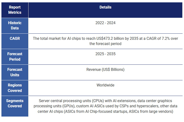
サマリー グラフィックス・プロセッシング・ユニット(GPU)、中央演算処理装置(CPU)、カスタムAI ASIC、その他のAIアクセラレータ、プレーヤー分析、テクノロジー、トレンド、サプライチェーン、および予測 フロンティアAIは、創薬や自律型インフラストラクチャのような領域で主導権を握ろうと各国政府やハイパースケーラーが競い合う中、世界規模で数千億ドルの投資を集めている。グラフィックス・プロセッシング・ユニット(GPU)やその他のAIチップは、データセンターやクラウド・インフラストラクチャ内でディープラーニングに必要な計算能力を提供し、人工知能のこの成長を推進する上で役立ってきた。GPUは、大規模言語モデル(LLM)やジェネレーティブAIという波の下流で支配的な下流として、計算能力を提供する上で極めて重要な役割を担ってきた。しかし、より効率的な計算、低コスト、高性能、大規模スケーラブルなシステム、より高速な推論、ドメインに特化した計算が求められる中、他のAIチップの人気が高まる機会がある。 IDTechExのレポート「データセンターとクラウド向けAIチップ 2025-2035年技術、市場、予測」は、AIチップの展望がGPUだけでなく、新アーキテクチャの広範な実用化に向けて広がっていることを伝えています:技術、市場、予測」は、データセンターとクラウド向けAIチップ市場を独自に分析しています。これには、現在および新興技術のベンチマーク、技術内訳、主要トレンドが含まれ、現在および新興のハードウェアアーキテクチャ、先進ノード技術、先進半導体パッケージングに加え、サプライチェーン、投資、政策に関する情報もカバーしています。データセンターとクラウドのAIチップ市場の2025年から2035年までのきめ細かな収益予測をAIチップのタイプ別に提供しています。これらには、GPU、ハイパースケーラーやクラウドサービスプロバイダー(CSP)が使用するカスタムAI特定用途向け集積回路(ASIC)、AI対応中央演算処理装置(CPU)、AIチップに特化した新興企業と大手ベンダーの両方が開発したその他のAI ASICが含まれる。 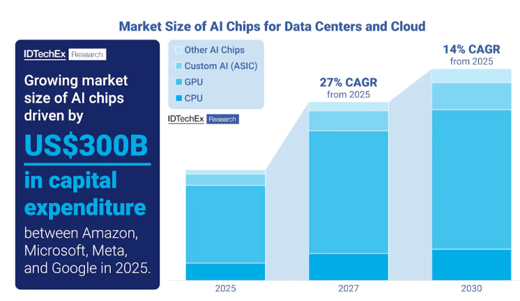 グラフィックス・プロセッシング・ユニット(GPU) AI向けの最大のシステムは、大規模なスケールアウトHPCおよびAIシステムであり、これらはGPUを大量に実装している。これらはハイパースケーラAIデータセンターとスーパーコンピュータであることが多く、オンプレミスまたは分散ネットワーク上でエクサフロップスのパフォーマンスを提供することができます。NVIDIAは近年、Hopper(H100/H200)チップや最近リリースされたBlackwell(B200/B300)チップで目覚ましい成功を収めている。AMDもMI300シリーズ・プロセッサー(MI300X/MI325X)で競争力のあるチップを開発した。また、先進的なチップに対する米国の制裁のため、中国のプレーヤーもソリューションを開発している。これらの高性能GPUは、最先端の半導体技術を採用し続けている。その一例がオンチップ・メモリ容量の増加で、トップ・チップは250GBを超える高帯域幅メモリ(HBM)を搭載しており、より多くのパラメータを持つ大規模なAIモデルをこれらのGPU上で実行できるようにしている。これらのチップはまた、TSMCのCoWoS-Lパッケージング、チップレット、マルチダイGPUなどの最先端の半導体パッケージングソリューションや、最先端のプロセスノード(5nm以下)を採用している。本レポートでは、これらすべてのトレンドと市場活動について詳しく解説する。 ハイパースケーラーとクラウドサービスプロバイダーが使用するカスタムAIチップ GPUはAIモデルのトレーニングに基本的な役割を果たしてきたが、総所有コスト(TCO)の高さ、ベンダーロックインのリスク、AI固有の操作に対する利用率の低さ、特定の推論ワークロードには過剰になりやすいなどの制約がある。ハイパースケーラーが採用しつつある新たな戦略は、シストリックアレイベースのカスタムAI ASICを使用することです。これらはAIワークロードのために専用に構築されたコアを持ち、演算単価が安く、特定のシステム(トランスフォーマー、レコメンダーシステムなど)に特化し、効率的な推論を提供し、ハイパースケーラーとCSPに性能を犠牲にすることなくフルスタックの制御と差別化の機会を与える。本レポートでは、潜在的なリスク、主要なパートナーシップ、プレイヤーの活動、ベンチマーク、技術概要の評価を掲載しています。 その他のAIチップ GPUをディスラプトするその他のAIチップは、類似のコンピューティング・アーキテクチャと斬新なコンピューティング・アーキテクチャの両方で製品化されている。Intel、Huawei、Qualcommなどの大手チップベンダーは、AIアクセラレータ(Gaudi、Ascend 910、Cloud AI 100など)を設計しており、ヘテロジニアス・アレイのコンピュート・ユニット(GPUに類似)を使用していますが、AIワークロードを高速化することを目的としています。これらのチップは、パフォーマンス、電力効率、および特定のアプリケーション・ドメインに対する柔軟性のバランスを提供する。多くの場合、これらのチップには行列エンジンとテンソルコアが搭載され、GEMM(一般行列乗算)やBMM(バッチ行列乗算)のような高密度線形代数演算を高いスループットで実行できるように設計されている。 AIチップに特化した新興企業は、データフロー制御プロセッサ、ウェハースケールパッケージング、空間AIアクセラレータ、PIM(Processing-in-Memory)技術、CGRA(Coarse-grained Reconfigurable Arrays)といった最先端のアーキテクチャや製造技術を導入し、異なるアプローチを取ることが多い。さまざまな企業がデータセンターやクラウド・コンピューティング向けにこれらのシステム(Cerebras、Groq、Graphcore、SambaNova、Untether AIなど)の立ち上げに成功しており、多くの場合、企業への導入が容易なラック規模のソリューションを開発したり、自社のクラウド・プラットフォームでの利用を提供している。これらのシステムは、特にスケールアップ環境において優れた性能を発揮する。IDTechExのレポートは、包括的なベンチマーク、比較、主要トレンド、技術内訳、プレーヤーの活動を提供している。 AIチップの設計とサプライチェーン 学習(time-to-train)と推論(tokens per second)のスループット、高いエネルギー効率(TOPS/watt)、関連するソフトウェアサポートで競争力のあるAIチップの開発は、すべてのチップ設計者にとって厳しい課題です。このプロセスには、プログラミングと実行モデルの選択、最適化されたハードウェアとメモリアーキテクチャの設計、先端プロセスノードと先端半導体パッケージによる製造など、多くのステップの絶妙なバランスが含まれます。例えば、データセンター・チップは、ASMLのEUV(極端紫外線)リソグラフィ技術を使用して、TSMC、インテル・ファウンドリ、サムスン・ファウンドリの最先端プロセス・ノードを採用しています。これらのファウンドリは、FinFET(フィン電界効果トランジスタ)を使用した5nm技術から、GAAFET(ゲートオールアラウンドFET)を使用した2nm以下のノードまで、バックサイド給電によるトランジスタ技術を押し上げています。最近の製造開発、デバイス要件、ハードウェアアーキテクチャの内訳、先端半導体パッケージの詳細、サプライチェーン、およびプログラミングモデルの比較はすべて、本レポートに含まれています。 設計と製造に関わる様々な技術により、半導体業界のサプライチェーン全体にわたって将来の技術革新の幅が広がっている。政府の政策と多額の投資は、フロンティアAIを新たな高みへと押し上げることへの関心の高さを示しており、この需要を満たすためにはAIデータセンター内でAIチップを大量に生産する必要がある。IDTechExは、この市場は2025年から2030年にかけて年平均成長率14%で成長し、売上高は4,000億米ドルを超えると予測している。 主要な側面 AIチップのハードウェア評価、ベンチマーク、比較
市場情報
市場予測と分析
目次
1. エグゼクティブサマリー
1.1. AIとは
1.2. データセンターおよびクラウド向けAIチップとは
1.3. AIモデルの性能がムーアの法則を超える中、AIチップは進化しなければならない
1.4. 大規模なAIモデルには、より多くのAIチップのスケーリングが必要
1.5. AIハードウェア市場の動向と戦略的変化
1.6. AIチップ設計のレイヤー
1.7. AIチップの種類
1.8. AIチップ技術の技術準備状況
1.9. ベンチマークされたAIチップ技術
1.10. AIチップランドスケープ - チップデザイナー
1.11. グラフィックス処理ユニット(GPU)
1.12. 高性能データセンターGPUのトレンド
1.13. AIワークロード加速のために主要なクラウドサービスプロバイダーが使用するASIC
1.14. AIデータセンターのGPU代替のトレンド
1.15. トレーニングおよび推論のためのAIチップの主要ワークロード
1.16. トレーニングおよび推論のハードウェア要求
1.17. 推論ベンチマーク:トップGPUのリアルタイム性能
1.18. 一般的なAIチップの性能:FP16/BF16精度
1.19. 過去10年間における先進的なプロセスノードとエネルギー効率のトレンド
1.20. 主要プレーヤー:AIチップ供給チェーン
1.21. 半導体産業に対する政府の産業政策および資金提供
1.22. アメリカのAIチップに対する中国への制裁
1.23. AIチップ市場規模予測:2025-2035年
1.24. GPU市場規模予測の注釈:2025-2035年
1.25. AIチップ採用の推進要因と課題
1.26. IDTechExサブスクリプションでさらにアクセス
2. AIモデルとAIチップの紹介
2.1.1. AIとは
2.1.2. AIチップとは
2.1.3. AI加速
2.1.4. AIチップ製品カテゴリの種類
2.1.5. 主要なAIチップ市場の概要
2.1.6. クラウドおよびデータセンターコンピューティング
2.1.7. クラウドおよびデータセンターコンピュータのユーザー、調達、パートナーシップ
2.1.8. クラウドAI
2.1.9. 企業コア
2.1.10. テレコムエッジ
2.1.11. エッジとクラウドの特徴
2.1.12. 主要プレーヤー:AIチップ供給チェーン
2.2. AIの基本
2.2.1. AIの基本:アルゴリズム、データ、ハードウェア
2.2.2. トレーニングと推論
2.2.3. AIチップは低精度計算を使用
2.2.4. AIチップでよく使用される数値表現
2.2.5. パラレルコンピューティング:データ並列性とモデル並列性
2.2.6. 深層学習:AIアルゴリズムの実装方法
2.2.7. ニューラルネットワークの説明
2.2.8. ニューラルネットワークの種類
2.2.9. ニューラルネットワークの種類と使用例
2.3. 大規模AIモデル
2.3.1. 2010年以降、パフォーマンスが年率4.5倍増加した注目のAIモデル
2.3.2. 自然言語処理においてRNNに代わりTransformerが使用される
2.3.3. 言語、コンピュータビジョン、マルチモーダルAIモデルが最も人気
2.3.4. AI性能がムーアの法則を超える理由
2.3.5. AIモデルの成長を支える主要な要因
2.3.6. システムのスケールアップおよびスケールアウト
2.3.7. AIモデルのトレーニングは非常にエネルギー集約的
2.3.8. 計算のハードウェア設計とエネルギー効率の非効率性
2.3.9. MLPerf Power:さまざまなAIチップタイプおよびアプリケーションにおける電力範囲
3. テクノロジー概説
3.1. AIチップのハードウェア設計概説
3.1.1. コンピュータハードウェアの歴史
3.1.2. AIハードウェアの進化
3.1.3. 予測されるAIチップのトレンド
3.1.4. AIチップ設計のレイヤー
3.2. 命令セットアーキテクチャ
3.2.1. AIワークロード向け命令セットアーキテクチャ(ISA)の紹介
3.2.2. AIアクセラレータ向けCISCおよびRISC ISA
3.3. プログラミングモデルと実行モデル
3.3.1. プログラミングモデルと実行モデル
3.3.2. フリンの分類法とプログラミングモデル
3.3.3. AIチップ向け重要な実行モデルとプログラミングモデル
3.3.4. フォン・ノイマンアーキテクチャの紹介
3.3.5. フォン・ノイマンと一般的なプログラミングモデルの比較
3.4. ハードウェアアーキテクチャ
3.4.1. ニューラルネットワークアーキテクチャに使用されるASIC、FPGA、およびGPU
3.4.2. AIチップのベンチマーク能力
3.4.3. AIチップの種類
3.4.4. AIチップ技術のTRL(技術準備レベル)
3.4.5. 商用AIチップの利点と欠点
3.4.6. 新興AIチップの利点と欠点
3.4.7. 一般的なプロセッサに見られる技術
3.4.8. 特殊目的リソース
3.4.9. アクセラレータ分類
3.5. トランジスタ
3.5.1. トランジスタの動作: p-n接合
3.5.2. ムーアの法則
3.5.3. 20nm以下の平面FETにおけるゲート長縮小の課題
3.5.4. トランジスタ数の増加
3.5.5. 平面FETからFinFETへの移行
3.5.6. GAAFET、MBCFET、RibbonFET
3.5.7. TSMCの先端ノードのロードマップ
3.5.8. インテルファウンドリの先端ノードのロードマップ
3.5.9. サムスンファウンドリの先端ノードのロードマップ
3.5.10. GAAFETスケーリング後に使用されるCFET
3.5.11. デバイスアーキテクチャのロードマップ (I)
3.5.12. スケーリング技術ロードマップの概要
3.6. 高度な半導体パッケージング
3.6.1. 1Dから3D半導体パッケージングへの進展
3.6.2. 高度な半導体パッケージング性能の主要な指標
3.6.3. 半導体パッケージングにおける相互接続技術の概要
3.6.4. 2.5Dパッケージング構造の概要
3.6.5. 2.5D高度な半導体パッケージング技術ポートフォリオ
3.6.6. 上位AIチップに使用される2.5D高度な半導体パッケージング
3.6.7. ダイサイズの制限の克服
3.6.8. 統合異種システム
3.6.9. ケーススタディ: AMD MI300A CPU/GPUの異種統合
3.6.10. 将来のシステムインパッケージアーキテクチャ
3.6.11. 高度な半導体パッケージングに関する詳細情報
4.1. CPUの技術概要
4.1.1. CPUの紹介
4.1.2. HPCおよびAI CPUのコアアーキテクチャ
4.1.3. HPCおよびAIワークロードに対する主要なCPU要件(1)
4.1.4. HPCおよびAIワークロードに対する主要なCPU要件(2)
4.1.5. x86-64命令セットのAVX-512ベクター拡張
4.2. インテルのCPU
4.2.1. インテル: データセンター向けXeon CPU
4.2.2. インテル: CPUにおけるAIアクセラレーションのためのAdvanced Matrix Extensions
4.2.3. インテル: AMXを活用した第4世代Xeonスケーラブルプロセッサのパフォーマンス
4.3. AMDのCPU
4.3.1. AMD: データセンター向けEPYC CPU
4.4. IBMのCPU
4.4.1. IBM: データセンター向けPower CPU
4.5. ArmのCPU
4.5.1. Arm: RISCベースのISAを使用したコアデザインのライセンス
4.5.2. Arm: データセンター向けCPU
4.5.3. CPUの見通し
もちろんです!以下が翻訳した目次です。
---
**5. グラフィックス処理ユニット(GPU)**
5.1. GPUの市場概要
5.1.1. AI GPUの種類
5.1.2. GPUの歴史的背景
5.1.3. 2010年代以降のGPUの人気
5.1.4. 地域別のデータセンターGPUプレイヤーの状況
5.1.5. 米国および中国の主要なデータセンターGPUメーカーの商業活動
5.1.6. ドライバー:技術進展と市場機会
5.1.7. ドライバー:エネルギー効率、パフォーマンス、インセンティブ、ブランドの強さ
5.1.8. 障壁:独占、市場競争、製品の複雑さ
5.1.9. 障壁:研究開発、顧客からの競争、市場の統合
5.1.10. スタートアップがGPU市場リーダーと競争する方法
5.2. GPU技術の詳細
5.2.1. CPUとGPUの主要なアーキテクチャの違い
5.2.2. 高性能データセンターGPUのアーキテクチャの詳細
5.2.3. データセンターGPUの主な特徴
5.2.4. NVIDIAとAMDのデータセンターGPUベンチマーク
5.2.5. 消費者向けGPUとしてのクラウドコンピュート
5.2.6. ワークステーション/プロフェッショナルGPUとしてのクラウドコンピュート
5.2.7. GPUの種類別価格
5.2.8. GPUのフォームファクターオプション
5.2.9. データセンターGPUフォームファクターの価格
5.2.10. スレッドがGPUとCPUによるレイテンシとスループットの処理方法を示す
5.2.11. NVIDIAとAMDのソフトウェア
5.2.12. 高性能データセンターGPUのトレンド
5.2.13. 高性能データセンターGPUのトレンド
5.3. NVIDIAのGPU
5.3.1. NVIDIA: テンソル数学
5.3.2. NVIDIA: テンソルコア
5.3.3. NVIDIA: NVIDIA CUDAとテンソルコア
5.3.4. NVIDIA: データセンターGPUの製品タイムライン
5.3.5. NVIDIA: Ampere GPU
5.3.6. NVIDIA: Hopper GPU
5.3.7. NVIDIA: Blackwell GPU(I)
5.3.8. NVIDIA: Blackwell GPU(II)
5.3.9. NVIDIA: ラックスケールソリューション
5.4. AMDのGPU
5.4.1. AMD: CDNA 3アーキテクチャとGPUコンピュート用コンピュートユニット
5.4.2. AMD: MI325X GPU
5.4.3. AMD: Instinct GPUと競争ポジショニング
5.4.4. AMD: MI300A CPU/GPUメモリの整合性と異種統合
5.5. インテルのGPU
5.5.1. インテル: Intel GPU Max とXe-HPCアーキテクチャ
5.5.2. インテル: 将来のASICおよび汎用GPU
5.6. 中国のGPU
5.6.1. Biren Technologies: 中国製GPGPU
5.6.2. Biren Technologies: BR100とBR104中国製GPGPU
5.6.3. Moore Threads: MTT S4000中国製GPU
5.6.4. MetaX: MXC500中国製GPGPU
5.6.5. Iluvatar CoreX: Tianyuan 100 とZhikai 100 中国製GPGPU
5.6.6. GPUの見通し
6. クラウドサービスプロバイダー(CSP)のカスタムAI ASIC
6.1. クラウドサービスプロバイダー向けカスタムAI ASICの市場概要
6.1.1. カスタムアプリケーション固有集積回路(ASIC)の紹介
6.1.2. アプリケーション別のAI ASIC
6.1.3. GPUと競争するために市場に登場したカスタムASIC
6.1.4. 投資のドライバーとカスタムASICの課題
6.1.5. 地域別のCSPカスタムASICプレイヤーの状況
6.1.6. AIワークロード加速のために主要クラウドサービスプロバイダーが使用するASIC
6.1.7. AI ASIC企業の能力
6.2. クラウドサービスプロバイダー向けカスタムAI ASICのハードウェア詳細
6.2.1. GPUとASICの比較
6.2.2. クラウドサービスプロバイダーのASICは同様のアーキテクチャを使用し、シストリックアレイを利用
6.2.3. ASICのシストリックアレイはGPUのテンソルコアの代替
6.2.4. 「シストリックアレイのロックイン」
6.3. 主要プレイヤー
6.3.1. Google TPU
6.3.2. Amazon: TrainiumとInferentia
6.3.3. Amazon: TrainiumとInferentiaのチップコンポーネントとパッケージング
6.3.4. Microsoft: Maia
6.3.5. Meta: MTIA
6.3.6. 将来の米国ASICプレイヤー
6.3.7. 中国のASICプレイヤーとクラウドサービスプロバイダーの中国製AIチップ
6.3.8. 見通し
7. その他のAIチップ
7.1.1. 他のアーキテクチャの紹介:章の概要
7.1.2. 他のAIチップのプレイヤーランドスケープ(地域別)
7.2. 異種マトリックス型AIアクセラレータ
7.2.1. 異種マトリックス型AIアクセラレータ
7.2.2. 異種マトリックス型AIアクセラレータのアーキテクチャ
7.2.3. ハバナ: Gaudi
7.2.4. インテル: Gaudi2
7.2.5. インテル: Greco
7.2.6. インテル: Gaudi3
7.2.7. カンブリコン・テクノロジーズ: Siyuan 370(中国のAIテンソルベースのAIチップ)
7.2.8. ファーウェイ: Ascend 910
7.2.9. ファーウェイ: Da Vinciアーキテクチャ
7.2.10. バイドゥ: KunlunおよびXPU
7.2.11. クアルコム: Cloud AI 100
7.2.12. クアルコム: AIコア
7.2.13. 主要プレイヤーの要約
7.3. 空間AIアクセラレータ
7.3.1. 空間AIアクセラレータ
7.3.2. セレブラス: ウェファースケールプロセッサ(GPUの競合)
7.3.3. セレブラス: WSE-3
7.3.4. サンバノバ: 再構成可能なデータフロー処理装置(GPUの代替)
7.3.5. サンバノバ: SN40L 再構成可能データフローユニット(RDU)
7.3.6. グラフコア: 第2世代Colossus™ MK2 IPUプロセッサ
7.3.7. グラフコア: Bow IPUとPods
7.3.8. グロック: AI推論用の自然言語プロセッサ
7.3.9. グロック: パフォーマンスと技術
7.3.10. アンテザーAI: SpeedAI240(メモリ内計算を使用)
7.3.11. 主要プレイヤーの要約(I)
7.3.12. 主要プレイヤーの要約(II)
7.4. 粗粒度再構成可能配列(CGRA)
7.4.1. CGRAは主流の計算基盤の未来の競争相手になる可能性
7.4.2. CGRAの内訳
7.4.3. 未来の展望 – 高エネルギー効率とパフォーマンスを持つ柔軟なアーキテクチャの探求
7.4.4. CGRA対データフロー対多コア
7.4.5. AIデータセンター向けGPUの代替技術の動向
7.4.6. その他のAIチップの動向
8. ベンチマークとハードウェアの動向
8.1. AIチップのベンチマーク
8.1.1. MLCommonsによるAIチップのベンチマーク(MLPerf)
8.1.2. MLCommonsベンチマーク:トレーニングと推論の主要ワークロードとモデル
8.1.3. AIチップの能力(I)
8.1.4. AIチップの能力(II)
8.1.5. トレーニングベンチマーク
8.1.6. 推論ベンチマーク
8.1.7. ベンチマークされたAIチップ技術
8.2. パフォーマンスとスケーラビリティ
8.2.1. MLPerf推論:データセンター:トークン/秒
8.2.2. MLPerfトレーニング:自然言語処理のパフォーマンス
8.2.3. MLPerfトレーニング:NVIDIAのパフォーマンス
8.2.4. MLPerfトレーニング:Google TPUのスケーラビリティ
8.2.5. NVIDIAとAMDのデータセンターGPUのスループット(OpenCLベンチマーク)
8.2.6. ネオクラウドジャイアンツ:GPU推論パフォーマンスとGPUスケーラビリティ
8.2.7. 一般的なAIチップのパフォーマンス:FP16/BF16精度
8.2.8. 一般的なAIチップのパフォーマンス:異なる精度の比較
8.3. エネルギー効率
8.3.1. 異なるAIチップのパフォーマンスあたりのワット
8.3.2. 過去10年間の高度なプロセスノードとエネルギー効率の動向
8.4. メモリとメモリ帯域幅
8.4.1. 主要課題:メモリ壁
8.4.2. メモリ壁の説明:メモリ階層の遅延ボトルネック
8.4.3. 異なるチップタイプのメモリ帯域幅
8.4.4. 高帯域幅メモリ(HBM)と他のDRAM技術との比較
8.4.5. HBM世代の進化とHBM4への移行
8.4.6. 主要プレイヤーによるHBM技術の市場ベンチマーク(1)
8.4.7. 主要プレイヤーによるHBM技術の市場ベンチマーク(2)
8.4.8. メモリ帯域幅の動向
8.4.9. メモリ容量の動向
8.5. 新しいAIアクセラレータのパフォーマンス評価時の考慮事項
8.5.1. AIアクセラレータのパフォーマンス評価
8.5.2. アクセラレータのパフォーマンスはさまざまな指標で測定する必要がある
8.5.3. レイテンシはさまざまな戦略で最適化する必要がある
8.5.4. 屋根ラインモデルを使用した豊富なデータ計算システムの基礎
8.5.5. ピークスループットはDNNアクセラレータ設計の制約によって制限される
8.5.6. 計算のハードウェア設計とエネルギー効率の非効率性
8.5.7. 幅広いDNNを処理するための柔軟性が重要
8.5.8. 学術的な例からのチップ間ネットワーク(NoC)の柔軟性
9. サプライチェーン、投資、貿易制限
9.1. サプライチェーン
9.1.1. ICサプライチェーンのプレイヤーカテゴリ
9.1.2. 集積回路サプライチェーンモデル
9.1.3. 生産プロセスによるサプライチェーン
9.1.4. AIチップサプライチェーンの集中
9.1.5. AIチップのためのサプライチェーンのポピュレーション
9.1.6. AIチップのためのコンポーネント別サプライチェーンのポピュレーション
9.1.7. AIチップランドスケープ - チップ設計者
9.1.8. カスタム集積回路のためのサプライチェーンのポピュレーション
9.1.9. IDM製造能力
9.1.10. ファウンドリ能力
9.1.11. AIクラウドカテゴリーとプレイヤー
9.1.12. 米国ハイパースケーラーの設備投資
9.2. 投資
9.2.1. 半導体産業のための政府の産業政策と資金援助
9.2.2. 米国と欧州の先進パッケージングへの政府投資
9.2.3. アジアのパッケージングとTSMCサプライチェーンへの政府投資
9. 貿易制限
9.3.1. 米国の中国およびその他の国々に対する先進的半導体に関する政策
9.3.2. 2022年10月7日、米国による中国技術への制裁
9.3.3. 2023年10月17日、米国によるAIチップへの制裁(I)
9.3.4. 2023年10月17日、米国によるAIチップへの制裁(II)
9.3.5. 中国におけるAIチップのコンプライアンス
9.3.6. 2024年12月2日、先進的コンピューティングおよび半導体製造に対するさらなる規制
9.3.7. 高帯域幅メモリ(HBM)への制限
9.3.8. 2025年1月13日、AI拡散フレームワーク(米国の世界的輸出規制)(I)
9.3.9. 2025年1月13日、AI拡散フレームワーク(米国の世界的輸出規制)(II)
9.3.10. 米国の制限の影響を受けたNVIDIAの収益(地域別)
10. 予測
10.1.1. 予測方法論
10.1.2. 予測の前提条件と見通し
10.1.3. AIチップ市場規模予測:2025-2035年
10.1.4. AIチップ市場シェア予測:2025-2035年
10.1.5. GPU市場規模予測注釈:2025-2035年
10.1.6. IDTechExのGPUに関する見通し
10.1.7. カスタムAI ASIC市場価値
10.1.8. カスタムAI ASICの市場規模予測注釈:2025-2035年
10.1.9. IDTechExのカスタムAI ASICチップに関する見通し
10.1.10. その他のAIチップ市場規模予測注釈:2025-2035年
10.1.11. IDTechExのその他のAIチップアーキテクチャに関する見通し

Summary
Graphics processing units (GPUs), central processing units (CPUs), custom AI ASICs, and other AI accelerators, with player analysis, technologies, trends, supply chain, and forecasts
Frontier AI attracts hundreds of billions in global investment, with governments and hyperscalers racing to lead in domains like drug discovery and autonomous infrastructure. Graphics processing units (GPUs) and other AI chips have been instrumental in driving this growth of artificial intelligence, providing the compute needed for deep learning within data centers and cloud infrastructure. GPUs have been pivotal in delivering computational capabilities, being the dominant undercurrent below the wave that is large language models (LLMs) and generative AI. However, with the demand for more efficient computation, lower costs, higher performance, massively scalable systems, faster inference, and domain-specific computation, there is opportunity for other AI chips to grow in popularity.
As the landscape of AI chips broadens past just GPUs, with novel architectures reaching widescale commercialization, IDTechEx's report "AI Chips for Data Centers and Cloud 2025-2035: Technologies, Market, Forecasts" offers an independent analysis of the AI chip market for data centers and the cloud. This includes benchmarking current and emerging technologies, technology breakdowns, and key trends, covering current and emerging hardware architectures, advanced node technologies, and advanced semiconductor packaging, as well as information on supply chain, investments, and policy. Granular revenue forecasts from 2025 to 2035 of the data center and cloud AI chips market are provided, segmented by types of AI chips. These include GPUs, custom AI application-specific integrated circuits (ASICs) used by hyperscalers and cloud service providers (CSPs), AI-capable central processing units (CPUs), and other AI ASICs developed by both AI chip-focused startups and large vendors.
Graphics Processing Units (GPUs)
The largest systems for AI are massive scale-out HPC and AI systems - these heavily implement GPUs. These tend to be hyperscaler AI data centers and supercomputers, both of which can offer exaFLOPS of performance, on-premise or over distributed networks. NVIDIA has seen remarkable success over recent years with its Hopper (H100/H200) chips and recently released Blackwell (B200/B300) chips. AMD has also created competitive chips with its MI300 series processors (MI300X/MI325X). Chinese players are also developing solutions due to sanctions from the US on advanced chips. These high-performance GPUs continue to adopt the most advanced semiconductor technologies. One example is increased on-chip memory capacity, with top chips having over 250GB of high-bandwidth memory (HBM), enabling larger AI models with even more parameters to run on these GPUs. These chips also adopt the most advanced semiconductor packaging solutions, such as TSMC's CoWoS-L packaging, chiplets, and multi-die GPUs, as well as the most advanced process nodes (5nm and below). All of these trends and market activities are explored in detail in this report.
Custom AI Chips Used by Hyperscalers and Cloud Service Providers
GPUs have been fundamental for training AI models but face limitations, such as high total cost of ownership (TCO), vendor lock-in risks, low utilization for AI-specific operations, and can be overkill for specific inference workloads. An emerging strategy that hyperscalers are adopting is using systolic array-based custom AI ASICs. These have purpose-built cores for AI workloads, are cheaper per operation, are specialized for particular systems (e.g., transformers, recommender systems, etc), offer efficient inference, and give hyperscalers and CSPs the opportunity for full-stack control and differentiation without sacrificing performance. Evaluation of potential risks, key partnerships, player activity, benchmarking, and technology overviews is available with this report.
Other AI Chips
Other AI chips are being commercialized to disrupt GPUs, with both similar and novel computing architectures. Some large chip vendors, such as Intel, Huawei, and Qualcomm, have designed AI accelerators (e.g., Gaudi, Ascend 910, Cloud AI 100), using heterogeneous arrays of compute units (similar to GPUs), but purpose-built to accelerate AI workloads. These offer a balance between performance, power efficiency, and flexibility for specific application domains. Often, these chips will contain matrix engines and tensor cores, which are designed to execute dense linear algebra operations like GEMM (General Matrix Multiply) and BMM (Batch Matrix Multiply) with high throughputs.
AI chip-focused startups often take a different approach, deploying cutting-edge architectures and fabrication techniques with the likes of dataflow-controlled processors, wafer-scale packaging, spatial AI accelerators, processing-in-memory (PIM) technologies, and coarse-grained reconfigurable arrays (CGRAs). Various companies have successfully launched these systems (Cerebras, Groq, Graphcore, SambaNova, Untether AI, and others) for data centers and cloud computing, often developing rack-scale solutions for easy enterprise deployment or offering usage on their own cloud platforms. These systems perform exceptionally, especially in scale-up environments. IDTechEx's report offers comprehensive benchmarking, comparisons, key trends, technology breakdowns, and player activity.
Designing AI chips and supply chain
Developing an AI chip with competitive throughput for training (time-to-train) and inference (tokens per second), high-energy efficiencies (TOPS/watt), and associated software support is a stringent challenge for all chip designers. This process involves a fine balance of many steps, including selecting programming and execution models, designing optimized hardware and memory architecture, and fabrication with advanced process nodes and advanced semiconductor packaging. For instance, data center chips are adopting the most advanced process nodes from TSMC, Intel Foundry, and Samsung Foundry, using EUV (extreme ultraviolet) lithography techniques from ASML. These foundries are pushing transistor technologies past 5nm technologies using FinFET (Fin-field effect transistor) to sub-2nm nodes using GAAFET (gate-all-around FETs) with backside power delivery. Recent fabrication developments, device requirements, hardware architecture breakdowns, advanced semiconductor packaging details, supply chain, and programming model comparisons are all included throughout this report.
The various technologies involved in designing and manufacturing give wide breadth for future technological innovation across the semiconductor industry supply chain. Government policy and heavy investment show the prevalent interest in pushing frontier AI toward new heights, and this will require exceptional volumes of AI chips within AI data centers to meet this demand. IDTechEx forecasts this market will grow at a CAGR of 14% from 2025 to 2030, with revenues exceeding US$400 billion.
Key Aspects
Hardware evaluation, benchmarking, and comparison for AI chips
Market information
Market forecast and analysis
Table of Contents1. EXECUTIVE SUMMARY
1.1. What is AI?
1.2. What are AI chips for data center and cloud?
1.3. AI chips must improve as performance of AI models outstrips Moore's Law
1.4. Large AI models require scaling of more AI chips
1.5. Market dynamics and strategic shifts in AI hardware
1.6. Layers to designing an AI chip
1.7. Types of AI Chips
1.8. Technology readiness of AI chip technologies
1.9. AI chip technologies benchmarked
1.10. AI chip landscape - Chip designers
1.11. Graphics Processing Units (GPUs)
1.12. Trends in high-performance data center GPUs
1.13. ASICs used by major cloud service providers for accelerating AI workloads
1.14. Trends in GPU alternatives for AI data center
1.15. AI chip key workloads for training and inference
1.16. Hardware demands for training and inference
1.17. Inference benchmarks show real time performance of top GPUs
1.18. Performance of common AI chips: FP16/BF16 precisions
1.19. Trends in advanced process nodes and energy efficiency in the last decade
1.20. Key players: AI chip supply chain
1.21. Government industrial policy and funding for semiconductor industry
1.22. US Sanctions on AI chips to China
1.23. Market size forecast of AI chips: 2025-2035
1.24. Annotated market size forecast of GPUs: 2025-2035
1.25. Drivers and challenges for AI chip adoption
1.26. Access More With an IDTechEx Subscription
2. INTRODUCTION TO AI MODELS AND AI CHIPS
2.1.1. What is AI?
2.1.2. What is an AI chip?
2.1.3. AI acceleration
2.1.4. Types of AI chip product categories
2.1.5. Overview of major AI chip markets
2.1.6. Cloud and data center computing
2.1.7. Users, procurement and partnerships of cloud and data center compute
2.1.8. Cloud AI
2.1.9. Enterprise core
2.1.10. Telecom edge
2.1.11. Edge vs Cloud characteristics
2.1.12. Key players: AI chip supply chain
2.2. Fundamentals of AI
2.2.1. Fundamentals of AI: Algorithms, Data, and Hardware
2.2.2. Training and inference
2.2.3. AI chips use low-precision computing
2.2.4. Common number representations in AI chips
2.2.5. Parallel computing: Data parallelism and model parallelism
2.2.6. Deep learning: how an AI algorithm is implemented
2.2.7. Neural networks explained
2.2.8. Types of Neural Networks
2.2.9. Types of neural networks and use cases
2.3. Large AI Models
2.3.1. Notable AI models increasing performance at a rate of 4.5x a year since 2010
2.3.2. Transformers used for LLM replace RNNs for natural language processing
2.3.3. Language, computer vision, and multimodal AI models are the most popular
2.3.4. Reasons for AI performance outpacing Moore's Law
2.3.5. Key drivers for continued growth of AI models
2.3.6. Scale-up and scale-out systems
2.3.7. Training AI models is very energy intensive
2.3.8. Hardware design and energy inefficiencies of compute
2.3.9. MLPerf Power: Power ranges for various AI chip types and applications
3. TECHNOLOGY OVERVIEW
3.1. AI Chips Hardware Design Overview
3.1.1. History of computer hardware
3.1.2. Progression of AI hardware
3.1.3. Trends in AI chips to expect
3.1.4. Layers to designing an AI chip
3.2. Instruction Set Architectures
3.2.1. Introduction to Instruction Set Architectures (ISAs) for AI workloads
3.2.2. CISC and RISC ISAs for AI accelerators
3.3. Programming Models and Execution Models
3.3.1. Programming model vs execution model
3.3.2. Flynn's taxonomy and programming models
3.3.3. Important execution models and programming models for AI chips
3.3.4. Introduction to Von Neumann Architecture
3.3.5. Von Neumann compared with common programming models
3.4. Hardware Architectures
3.4.1. ASICs, FPGAs, and GPUs used for neural network architectures
3.4.2. Benchmarking capabilities of AI chips
3.4.3. Types of AI Chips
3.4.4. TRL of AI chip technologies
3.4.5. Pros and cons of commercial AI chips
3.4.6. Pros and cons of emerging AI chips
3.4.7. Technologies found in general-purpose processors
3.4.8. Special-purpose resources
3.4.9. Accelerator taxonomy
3.5. Transistors
3.5.1. How transistors operate: p-n junctions
3.5.2. Moore's law
3.5.3. Gate length reductions pose challenges to planar FETs below 20nm
3.5.4. Increasing Transistor Count
3.5.5. Planar FET to FinFET
3.5.6. GAAFET, MBCFET, RibbonFET
3.5.7. TSMC's leading-edge nodes roadmap
3.5.8. Intel Foundry's leading-edge nodes roadmap
3.5.9. Samsung Foundry's leading-edge nodes roadmap
3.5.10. CFETs to be used beyond GAAFET scaling
3.5.11. Device architecture roadmap (I)
3.5.12. Scaling technology roadmap overview
3.6. Advanced Semiconductor Packaging
3.6.1. Progression from 1D to 3D semiconductor packaging
3.6.2. Key metrics for advanced semiconductor packaging performance
3.6.3. Overview of interconnection technique in semiconductor packaging
3.6.4. Overview of 2.5D packaging structure
3.6.5. 2.5D advanced semiconductor packaging technology portfolio
3.6.6. 2.5D advanced semiconductor packaging used in top AI chips
3.6.7. Overcoming die size limitations
3.6.8. Integrated heterogeneous systems
3.6.9. Case study: AMD MI300A CPU/GPU heterogenous integration
3.6.10. Future system-in-package architecture
3.6.11. For more information on advanced semiconductor packaging
4. AI-CAPABLE CENTRAL PROCESSING UNITS (CPUS)
4.1. Technology Overview of CPUs
4.1.1. CPU introduction
4.1.2. Core architecture of a HPC and AI CPU
4.1.3. Key CPU requirements for HPC and AI workloads (1)
4.1.4. Key CPU Requirements for HPC and AI Workloads (2)
4.1.5. AVX-512 vector extensions for x86-64 Instruction Set
4.2. Intel CPUs
4.2.1. Intel: Xeon CPUs for data center
4.2.2. Intel: Advanced Matrix Extensions in CPUs for built-in AI acceleration
4.2.3. Intel: 4th Gen Xeon Scalable Processor performance with AMX
4.3. AMD CPUs
4.3.1. AMD: EPYC CPUs for data center
4.4. IBM CPUs
4.4.1. IBM: Power CPUs for data center
4.5. Arm CPUs
4.5.1. Arm licenses core designs with its RISC-based ISAs
4.5.2. Arm CPUs for data center
4.5.3. CPU outlook
5. GRAPHICS PROCESSING UNITS (GPUS)
5.1. Market Overview of GPUs
5.1.1. Types of AI GPUs
5.1.2. Historical background of GPUs
5.1.3. GPUs popularity since the 2010s
5.1.4. Data center GPU player landscape by region
5.1.5. Commercial activity of key US and Chinese data center GPU manufacturers
5.1.6. Drivers: Technology advancements and market opportunities
5.1.7. Drivers: Energy efficiency, performance, incentives, and brand strength
5.1.8. Barriers: Monopolization, competition, and product complexity
5.1.9. Barriers: R&D, competition from customers, market consolidation
5.1.10. How can startups compete with GPU market leaders
5.2. GPU Technology Breakdown
5.2.1. Key architectural differences between CPUs and GPUs
5.2.2. Architecture breakdown of high-performance data center GPUs
5.2.3. Data center GPUs key features
5.2.4. NVIDIA and AMD data center GPUs benchmark
5.2.5. Consumer GPUs as cloud compute
5.2.6. Workstation / professional GPUs as cloud compute
5.2.7. Pricing of GPUs by type
5.2.8. Form factor options for GPUs
5.2.9. Pricing of data center GPU form factors
5.2.10. Threads show how latency and throughput is handled by GPUs and CPUs
5.2.11. NVIDIA and AMD software
5.2.12. Trends in high-performance data center GPUs
5.2.13. Trends in high-performance data center GPUs
5.3. NVIDIA GPUs
5.3.1. NVIDIA: Tensor mathematics
5.3.2. NVIDIA: Tensor cores
5.3.3. NVIDIA: NVIDIA CUDA and tensor cores
5.3.4. NVIDIA: Data center GPU product timeline
5.3.5. NVIDIA: Ampere GPUs
5.3.6. NVIDIA: Hopper GPUs
5.3.7. NVIDIA: Blackwell GPUs (I)
5.3.8. NVIDIA: Blackwell GPU (II)
5.3.9. NVIDIA: Rack-scale solutions
5.4. AMD GPUs
5.4.1. AMD: CDNA 3 Architecture and Compute Units for GPU Compute
5.4.2. AMD: MI325X GPU
5.4.3. AMD: Instinct GPU and competitive positioning
5.4.4. AMD: MI300A CPU/GPU memory coherency with heterogenous integration
5.5. Intel GPUs
5.5.1. Intel: Intel GPU Max and the Xe-HPC Architecture
5.5.2. Intel: Future ASIC and general-purpose GPU
5.6. Chinese GPUs
5.6.1. Biren Technologies: Chinese GPGPU
5.6.2. Biren Technologies: BR100 and BR104 Chinese GPGPU
5.6.3. Moore Threads: MTT S4000 Chinese GPU
5.6.4. MetaX: MXC500 Chinese GPGPU
5.6.5. Iluvatar CoreX: Tianyuan 100 and Zhikai 100 Chinese GPGPUs
5.6.6. GPU Outlook
6. CUSTOM AI ASICS FOR CLOUD SERVICE PROVIDERS (CSPS)
6.1. Market Overview of Custom AI ASICs for CSPs
6.1.1. Introduction to custom application-specific integrated circuits (ASICs)
6.1.2. AI ASICs based on application
6.1.3. Custom ASICs enter the market to compete with GPUs
6.1.4. Drivers for investment, and challenges for custom ASICs
6.1.5. CSP custom ASIC player landscape by region
6.1.6. ASICs used by major cloud service providers for accelerating AI workloads
6.1.7. AI ASIC companies' capabilities
6.2. Hardware Breakdown of Custom AI ASICs for CSPs
6.2.1. GPU and ASIC comparison
6.2.2. Cloud service provider ASICs have similar architectures, using systolic arrays
6.2.3. Systolic arrays in ASICS are an alternative to tensor cores in GPUs
6.2.4. "Systolic array lock-in"
6.3. Key Players
6.3.1. Google TPU
6.3.2. Amazon: Trainium and Inferentia
6.3.3. Amazon: Trainium and Inferentia chip components and packaging
6.3.4. Microsoft: Maia
6.3.5. Meta: MTIA
6.3.6. Future US ASIC players
6.3.7. Chinese ASIC players and Chinese AI chips from cloud service providers
6.3.8. Outlook
7. OTHER AI CHIPS
7.1.1. Introduction to other architectures: Chapter Overview
7.1.2. Other AI chips player landscape by region
7.2. Heterogenous Matrix-Based AI Accelerators
7.2.1. Heterogenous matrix-based AI accelerators
7.2.2. Heterogenous matrix-based AI accelerators architectures
7.2.3. Habana: Gaudi
7.2.4. Intel: Gaudi2
7.2.5. Intel: Greco
7.2.6. Intel: Gaudi3
7.2.7. Cambricon Technologies: Siyuan 370 is China's AI tensor-based AI chip
7.2.8. Huawei: Ascend 910
7.2.9. Huawei: Da Vinci architecture
7.2.10. Baidu: Kunlun and XPU
7.2.11. Qualcomm: Cloud AI 100
7.2.12. Qualcomm: AI core
7.2.13. Summary of key players
7.3. Spatial AI Accelerators
7.3.1. Spatial AI accelerators
7.3.2. Cerebras: Wafer-scale processors as a competitor to GPUs
7.3.3. Cerebras: WSE-3
7.3.4. SambaNova: Reconfigurable dataflow processors as substitute to GPUs
7.3.5. SambaNova: SN40L Reconfigurable Dataflow Unit (RDU)
7.3.6. Graphcore: Second-generation Colossus™ MK2 IPU processor
7.3.7. Graphcore: Bow IPU and Pods
7.3.8. Groq: Natural language processor designed for AI inference
7.3.9. Groq: Performance and technology
7.3.10. Untether AI: SpeedAI240 uses at-memory computation
7.3.11. Key players summary (I)
7.3.12. Key players summary (II)
7.4. Coarse-Grained Reconfigurable Arrays (CGRAs)
7.4.1. CGRAs could be a future contender for mainstream compute fabrics
7.4.2. CGRA breakdown
7.4.3. Future outlook - the search for flexible architectures with high energy efficiency and performance
7.4.4. CGRAs vs dataflow vs manycore
7.4.5. Trends in GPU alternatives for AI data center
7.4.6. Trends in other AI chips
8. BENCHMARKS AND HARDWARE TRENDS
8.1. Benchmarking AI Chips
8.1.1. MLPerf by MLCommons for benchmarking AI chips
8.1.2. MLCommons benchmarks: Training and inference key workloads and models
8.1.3. AI chip capabilities (I)
8.1.4. AI chip capabilities (II)
8.1.5. Training benchmarking
8.1.6. Inference benchmarking
8.1.7. AI chip technologies benchmarked
8.2. Performance and Scalability
8.2.1. MLPerf Inference: Data Center: Tokens per second
8.2.2. MLPerf Training: Natural Language Processing performance
8.2.3. MLPerf Training: NVIDIA performance
8.2.4. MLPerf Training: Scalability of Google TPUs
8.2.5. NVIDIA and AMD data center GPU throughput with OpenCL benchmark
8.2.6. Neocloud giants: GPU inference performance and GPU scalability
8.2.7. Performance of common AI chips: FP16/BF16 precisions
8.2.8. Performance of common AI chips: Comparing different precisions
8.3. Energy Efficiency
8.3.1. Performance per watt for different AI chips
8.3.2. Trends in advanced process nodes and energy efficiency in the last decade
8.4. Memory and Memory Bandwidth
8.4.1. Key challenge: The memory wall
8.4.2. Illustrating the memory wall: Memory hierarchy latency bottleneck
8.4.3. Memory bandwidths of different chip types
8.4.4. High bandwidth memory (HBM) and comparison with other DRAM technologies
8.4.5. Evolution of HBM generations and transition to HBM4
8.4.6. Benchmarking of HBM technologies in the market from key players (1)
8.4.7. Benchmarking of HBM technologies in the market from key players (2)
8.4.8. Memory bandwidth trends
8.4.9. Memory capacity trends
8.5. Considerations for Evaluating Performance of New AI Accelerators
8.5.1. Evaluating performance of AI accelerators
8.5.2. Performance of accelerators must be measured across various metrics
8.5.3. Latency must be optimized through various strategies
8.5.4. Fundamentals abundant data computing systems using the Roofline Model
8.5.5. Peak throughput is limited by DNN accelerator design constraints
8.5.6. Hardware design and energy inefficiencies of compute
8.5.7. Flexibility is key for handling wide range of DNNs
8.5.8. Network on Chip - example from academia showing flexibility
9. SUPPLY CHAIN, INVESTMENTS, AND TRADE RESTRICTIONS
9.1. Supply Chain
9.1.1. IC supply chain player categories
9.1.2. Integrated circuit supply chain models
9.1.3. Supply chain by production process
9.1.4. Concentration of AI chip supply chain
9.1.5. Populated supply chain for AI chips
9.1.6. Populated supply chain for AI chips by component
9.1.7. AI chip landscape - Chip designers
9.1.8. Populated supply chain for custom integrated circuits
9.1.9. IDM fabrication capabilities
9.1.10. Foundry capabilities
9.1.11. AI cloud categories and players
9.1.12. US hyperscalers capital expenditure
9.2. Investments
9.2.1. Government industrial policy and funding for semiconductor industry
9.2.2. Government investments in US and European advanced packaging
9.2.3. Government investments in Asian packaging and the TMSC supply chain
9.3. Trade Restrictions
9.3.1. US policy regarding advanced semiconductors in China and other nations
9.3.2. Oct 7th, 2022 US sanctions on China technologies
9.3.3. Oct 17th, 2023, US sanctions on AI chips (I)
9.3.4. Oct 17th, 2023, US sanctions on AI chips (II)
9.3.5. AI chips compliant in China
9.3.6. Dec 2nd, 2024, further controls on advanced computing and semiconductor manufacture
9.3.7. Restrictions on High-Bandwidth Memory (HBM)
9.3.8. Jan 13th, 2025, AI Diffusion Framework (US worldwide export controls) (I)
9.3.9. Jan 13th, 2025, AI Diffusion Framework (US worldwide export controls) (II)
9.3.10. NVIDIA revenues by geography, affected by US restrictions
10. FORECASTS
10.1.1. Forecast methodology
10.1.2. Forecast assumptions and outlook
10.1.3. Market size forecast of AI chips: 2025-2035
10.1.4. Market share forecast of AI chips: 2025-2035
10.1.5. Annotated market size forecast of GPUs: 2025-2035
10.1.6. IDTechEx outlook for GPUs
10.1.7. Custom AI ASIC market value
10.1.8. Annotated market size forecast of custom AI ASICs: 2025-2035
10.1.9. IDTechEx outlook for custom AI ASIC chips
10.1.10. Annotated market size forecast of other AI chips: 2025-2035
10.1.11. IDTechEx outlook for other AI chip architectures
ご注文は、お電話またはWEBから承ります。お見積もりの作成もお気軽にご相談ください。本レポートと同分野(半導体)の最新刊レポート
IDTechEx社の 半導体、コンピュータ、AI - Semiconductors, Computing & AI分野 での最新刊レポート
よくあるご質問IDTechEx社はどのような調査会社ですか?IDTechExはセンサ技術や3D印刷、電気自動車などの先端技術・材料市場を対象に広範かつ詳細な調査を行っています。データリソースはIDTechExの調査レポートおよび委託調査(個別調査)を取り扱う日... もっと見る 調査レポートの納品までの日数はどの程度ですか?在庫のあるものは速納となりますが、平均的には 3-4日と見て下さい。
注文の手続きはどのようになっていますか?1)お客様からの御問い合わせをいただきます。
お支払方法の方法はどのようになっていますか?納品と同時にデータリソース社よりお客様へ請求書(必要に応じて納品書も)を発送いたします。
データリソース社はどのような会社ですか?当社は、世界各国の主要調査会社・レポート出版社と提携し、世界各国の市場調査レポートや技術動向レポートなどを日本国内の企業・公官庁及び教育研究機関に提供しております。
|
|