シリコンフォトニクスおよびフォトニック集積回路 2026-2036:技術、市場、および予測Silicon Photonics and Photonic Integrated Circuits 2026-2036: Technologies, Markets, and Forecasts 化合物半導体、トランシーバー、リン化インジウム(InP)PIC、ニオブ酸リチウム薄膜(TFLN)PIC、量子技術向けPIC、光インターコネクト、製造、材料、コパッケージド・オプティクス、マイクロLED AIが... もっと見る

サマリー化合物半導体、トランシーバー、リン化インジウム(InP)PIC、ニオブ酸リチウム薄膜(TFLN)PIC、量子技術向けPIC、光インターコネクト、製造、材料、コパッケージド・オプティクス、マイクロLED
AIがフォトニクス革命を牽引している
現代の AI や高性能コンピューティングのワークロードでは、チップ、サーバー、ラック間で膨大な量の情報を驚異的な速度で伝送する必要があります。 従来は銅配線でこれに対応してきましたが、現在の世代のアーキテクチャでは銅配線が達成できる物理的な限界に近づきつつあり、業界はいわゆる「相互接続のボトルネック」に直面しています。これは、生の演算能力が相互接続の帯域幅を上回り、非常に高価で消費電力の大きいアクセラレータチップが、有用なトレーニングや推論を行うのではなく、データを待つだけでアイドル状態になってしまうという状況です。
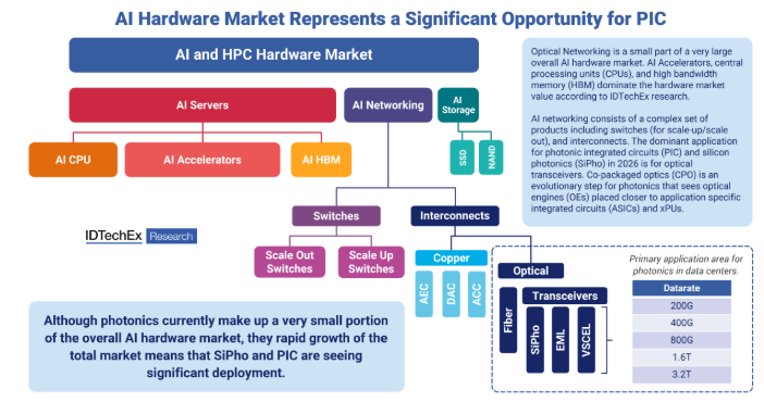
フォトニック・ネットワーキングは、AIハードウェアに対する市場全体の需要のうち、規模は小さいものの重要な部分を占めています。出典:IDTechEx
業界の解決策は、光通信への移行であり、銅線内の電子の代わりに光子を利用してデータを伝送することです。光子は速度が速く、信号損失が少なく、高度な変調技術を用いることでより高いデータ転送速度を実現できます。フォトニック集積回路(PIC)は、単一のチップ上で電気信号と光信号の処理を可能にする光電気システムであり、光子の固有の利点と半導体産業の巨大なスケールメリットを融合させたものです。 究極の目標は、光の生成、処理、変調、検出をすべてシリコンチップ上で行うモノリシック・シリコン・チップの実現です。しかし、シリコンは間接バンドギャップ半導体であるため、純粋なシリコンレーザーの構築は不可能です。この単純な物理的制約が、様々な材料プラットフォーム、集積技術、設計を備えたフォトニクス産業全体の発展を促進してきました。IDTechExによる本レポートは、この急速に進化する産業について明確な理解と洞察を提供することを目的としています。
今日のPIC産業の主な牽引役は光トランシーバーである
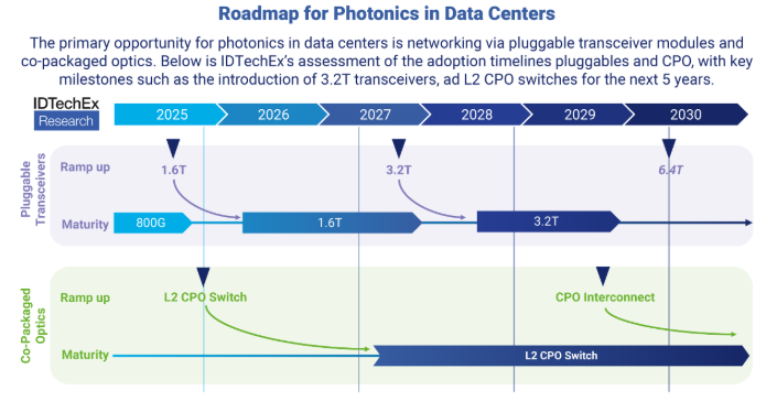
データセンター全体での情報伝送は光技術の領域ですが、チップ内部では依然として電子が支配的です。光トランシーバーは電気信号と光信号の相互変換を担っており、IDTechExの調査によると、PICの「キラーアプリケーション」として台頭し、業界を脚光を浴びる存在へと押し上げています。 データ転送速度は数年ごとに倍増しており、2026年には毎秒1.6テラビットの光トランシーバーが商用化されました。これにより、最新世代のアクセラレータアーキテクチャにおいて、高帯域幅かつ低遅延のチップ間通信が可能になりました。IDTechExは、このデータ転送速度の倍増傾向が続くと見込んでおり、2020年代末には3.2Tトランシーバーが登場すると予測しています。
CPOの成功にはフォトニクスが不可欠
データレートが上昇するにつれ、最終的には光エンジンとASIC(特定用途向け集積回路)間の短い銅配線さえも、性能のボトルネックとなり始めます。その解決策の鍵は、光エンジンをASICに大幅に近づけ、同一基板上にパッケージングすることにあります。 これを実現するため、フォトニクス業界は、発熱するASICとレーザーを統合するという厳しい熱要件を満たすよう設計された、一連のシリコンフォトニック変調器および超高出力レーザーを開発してきました。本レポートでは、TSMCのCOUPEプラットフォームや、CPO対応のUHP(超高出力)レーザーの商用化をめぐる競争など、主要なソリューションについて詳しく掘り下げています。
データセンター・ネットワーキングにおけるフォトニクスの導入ロードマップに関するIDTechExの評価(光トランシーバーおよびコパッケージド・オプティクスの両方)。出典:IDTechEx。
現在のPIC材料と将来の展望とは?
ほぼ完全にシリコンで構成される従来の論理集積回路とは異なり、PICには利用可能な材料プラットフォームの多様性がはるかに大きい。現在の市場の大部分では、光伝搬にシリコンおよびシリカベースのPICが使用されている。しかし、間接バンドギャップ半導体であるシリコンは、実用的な光源や光検出器としては適していない。そのため、光源や光検出には通常、シリコンがIII-V族材料(一般的にはリン化インジウム)と組み合わされる。 業界が進化する中、IDTechExは薄膜ニオブ酸リチウム(TFLN)を含む、注目すべきいくつかのプラットフォームを特定しました。適度なポッケルス効果と低い材料損失を特徴とするTFLNは、量子システムや将来の高性能トランシーバーなど、高性能な変調を必要とするアプリケーションにおいて有力な候補として台頭しています。 モノリシックインジウムリン(InP)は、光を検出し発光する能力を持つため、引き続き主要な材料としての地位を維持しています。さらに、チタン酸バリウム(BTO)や希土類金属といった革新的な材料も、量子コンピューティングやその他の最先端用途における可能性を秘めているとして、研究が進められています。
新しい回路と新しいサプライチェーン
データ通信におけるフォトニクス革命は、全く新しいエコシステムの発展を後押ししています。 IC設計会社、ファウンドリ、OSAT(外注組立・試験)など、いくつかのプロセスはロジック半導体産業と類似しています。PICおよびPICベースのトランシーバーには、レーザー、フォトダイオード、光ファイバーなど、数多くの新しい部品も必要となります。また、信号損失を最小限に抑え、正しい機能を確保するためにサブミクロンレベルの精度が求められるため、光アライメントとパッケージングも重要な工程として浮上しています。 インジウム・フォスファイド(InP)は、InPモノリシック・トランシーバーやシリコンフォトニクスにおける光源として不可欠な材料ですが、その原料となるインジウムの生産は、亜鉛製造の副産物として中国に高度に集中しています。需要の拡大に伴い生産は拡大しており、一部の企業(Coherentなど)は6インチInPウェハーの生産を開始しています。
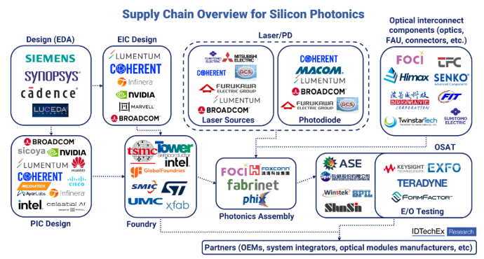
IDTechExによる本レポートは、シリコンフォトニクス・エコシステムの新たなサプライチェーンを追跡しています。出典:IDTechEx。
世界の製造動向も変化しており、東南アジアが中国および米国のトランシーバーメーカー双方にとっての製造拠点として台頭している一方、ハイエンドのレーザー部品は依然として米国および日本のエレクトロニクス大手企業の領域となっています。本レポートは、フォトニクス産業の新たなエコシステムとサプライチェーンを分析し、バリューチェーンのあらゆる段階にあるユーザーに深い洞察を提供することを目的としています。
IDTechExによる本レポートは、2026年におけるPIC(光集積回路)の、新興かつダイナミックなエコシステムとサプライチェーンを追跡しています。
将来の応用分野は?
シリコンフォトニクスおよびPICのその他の応用分野は多岐にわたり、高帯域幅のチップ間相互接続から、先進的なパッケージングやコパッケージド・オプティクス(CPO)に至るまで様々です。これらの技術は、次世代コンピューティングへの道を開いています。特にCPOは、スケールアップおよびスケールアウト型ネットワークに向けた、より高度な光集積を実現する将来の手法として注目を集めています。
開発のかなり初期段階にあるのが、まだ揺籃期にある量子技術市場です。多くの企業がトラップドイオンおよび光子ベースの量子コンピューティングに投資しており、より安定的でスケーラブルな量子システムを実現するためのPICを求めています。課題は、量子計算に必要な光子の精密な制御を実現することにあります。 量子センサーもPICを活用可能です。例えば、光原子時計、光励起磁力計(OPM)、重力計、量子ジャイロスコープなどが挙げられます。本レポートでは、量子技術におけるフォトニック集積回路の応用、材料、および課題に焦点を当てています。
PICおよびSiPho市場の推移
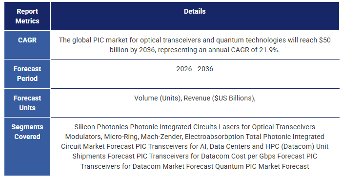
IDTechExによると、データ通信および量子技術向けの光トランシーバー用フォトニック集積回路(PIC)およびシリコンフォトニクス市場は、2036年までに500億ドルに達し、21.9%という堅調な年平均成長率(CAGR)を示すと予測されています。 市場価値の大部分は、高度なコンピューティングアプリケーションにおける高速データ処理および通信への需要増に対応するための、PICベースの光トランシーバーによってもたらされる見込みです。様々な量子技術向けのPICは、予測期間の後半に、規模は小さいながらも重要な収益の牽引役として台頭するでしょう。
IDTechExの最新レポート『シリコンフォトニクスおよびフォトニック集積回路 2026-2036:技術、市場、予測』は、PIC技術の最新の進展について詳細な評価を提供しています。 本レポートでは、フォトニクス向けの変調器、光源、導波路、材料プラットフォームなどの主要技術やコンポーネントを包括的に分析するとともに、サプライチェーン、市場動向、および最終用途アプリケーションを評価しています。 また、MicroLED相互接続技術がもたらす新たな「ワイド・アンド・スロー(wide-and-slow)」アーキテクチャについても評価しています。包括的かつ詳細な市場予測とアナリストの見解を提供し、今後10年間にわたるフォトニクス市場の進化に関するIDTechExの見解を示しています。
主な内容:
本レポートは、シリコンフォトニクスおよびフォトニック集積回路(PIC)市場に関する包括的な分析を提供します。本レポートでは、以下のトピックを網羅しています
本レポートは、広範な調査および業界専門家へのインタビューに基づいており、フォトニック集積回路の将来に関心のあるすべての人々に貴重な洞察を提供します。
市場予測
目次
1. エグゼクティブ・サマリー
1.1. 前回版以降のフォトニクス業界における主要な取引
1.2. シリコンフォトニクスの定義
1.3. フォトニック集積回路(PIC)とは?
1.4. フォトニック集積回路の利点と課題
1.5. PICの集積化手法
1.6. PIC材料プラットフォームの比較評価(可視化)
1.7. フォトニック集積回路の主要構成要素
1.8. レーザーの選択肢の概要
1.9. フォトニック集積回路用変調器
1.10. シリコンフォトニクスのサプライチェーン概要
1.11. InPフォトニクスのサプライチェーン概要
1.12. 光モジュールの製造能力が東南アジアへシフト( )
1.13. フォトニック集積回路の主要な現在および将来の応用分野
1.14. AIハードウェア市場はPICにとって大きな機会となる
1.15. 銅の壁
1.16. データセンターにおけるフォトニクスのロードマップ
1.17. ハイエンドデータセンターにおける光トランシーバーの主要トレンド
1.18. マイクロLED光インターコネクトのアプリケーション動向
1.19. アナリストの見解:データセンター・ネットワーキングにおいてフォトニクスは不可避か?
1.20. データ通信用PICトランシーバーの材料展望
1.21. 量子技術におけるフォトニクス、シリコンフォトニクス、および光学の概要
1.22. 量子PIC市場予測
1.23. 本レポートに含まれる企業プロファイルおよび記事
1.24. IDTechExのサブスクリプションでさらに多くの情報にアクセス
2. 序論および主要概念
2.1.1. シリコンフォトニクスの定義
2.1.2. PICとシリコンフォトニクスの違いとは?
2.2. 技術の背景
2.2.1. 集積回路(IC)とは何か?
2.2.2. フォトニック集積回路(PIC)とは何か?
2.2.3. フォトニクスとエレクトロニクスの比較
2.2.4. 電子集積回路とフォトニック集積回路の比較
2.2.5. フォトニック集積回路の利点と課題
2.2.6. シリコン集積回路とフォトニック集積回路
2.2.7. PICの主な利点
3. フォトニック集積回路の主要構成要素
3.1. フォトニック集積回路の主要構成要素に対する要件
3.2. フォトニック集積回路の主要構成要素
3.3. シリコンフォトニクス・トランシーバーの構成要素の内訳
3.4. TSMCのCoupe PDK
4. 光源および検出器
4.1. 発光および光子源/レーザー
4.2. 化合物半導体レーザーおよび光検出器(III-V系)
4.3. 光学材料の動作周波数帯域
4.4. レーザーの選択肢の概要
4.5. エッジ発光レーザー(EEL)
4.6. 垂直共振器面発光レーザー(VCSEL)
4.7. CPO UHPレーザーの要件
4.8. レーザー技術の概要
4.9. EMLの供給不足がSiPhoへの移行を促進
4.10. のサプライチェーン - フォトダイオード(PD)およびレーザー
4.11. の主要レーザーチップサプライヤー:Lumentum対Coherent
4.12. :レーザー技術に関するアナリストの見通し
4.13. の検出および光検出器
5. 変調器
5.1. フォトニック集積回路用 変調器
5.2. 変調器技術の概要
5.3. マッハ・ゼンダー変調器 - トランシーバーの主流技術
5.4. MRMs-TSMCとNVIDIAにとっての新たな競争優位性となるか?
5.5. セレスティアル・マーベル社との提携 - SiGe EAM
5.6. Tower SemiとLightwaveのEOポリマー
6. 受動デバイス
6.1. のPICアーキテクチャ
6.2. の光伝搬と導波路
6.3. 導波路の材料設計におけるトレードオフ
6.4. 導波路用材料の選択肢
6.5. 光I/O、結合およびカプラ
6.6. 光学部品の密度
7. 材料および製造
7.1.1. ウェハー
7.1.2. プラットフォーム別 ウェハサイズ
7.1.3. 集積化手法
7.1.4. 異種集積技術の比較:
7.1.5. InPおよびシリコンフォトニクスの異種集積のための マイクロ転写印刷
7.1.6. 光学材料の動作周波数帯域
7.1.7. 重要な波長・周波数のまとめ
7.1.8. PICにおける材料の挙動の変化
7.1.9. PICを開発する研究機関およびPIC専門ファウンドリ (1)
7.1.10. PICを開発している研究機関およびPIC専用ファウンドリ(2)
7.1.11. PICを開発する研究機関およびPIC専用ファウンドリ (3)
7.1.12. 欧州の産業コンソーシアムおよび協会
7.1.13. PhotonixFABコンソーシアム
7.1.14. シリコンおよびシリコン・オン・インシュレータ(SOI)
7.1.15. シリコンフォトニクスのサプライチェーン概要
7.1.16. SOIのベンチマーク
7.1.17. CEA-Letiおよびimecによる最新のSOI PIC開発
7.1.18. 窒化ケイ素(SiN)
7.1.19. SiN PICの主要企業
7.1.20. SiN主要ファウンドリ
7.1.21. SiNのベンチマーク
7.1.22. シリコン(SOIおよびSiN)デバイスのヘテロジニアス統合
7.1.23. リン化インジウム
7.1.24. リン化インジウムの既存集積技術 (1)
7.1.25. リン化インジウムの既存集積技術 (2)
7.1.26. InP ベンチマーク
7.1.27. シリコン上の有機ポリマー
7.1.28. ケーススタディ:有機ポリマー PIC の製造方法(Lightwave Logic)
7.1.29. 絶縁体上ポリマー( )のベンチマーク
7.1.30. ニオブ酸リチウム薄膜
7.1.31. TFLNの製造方法
7.1.32. TFLNの集積化と形状
7.1.33. TFLNのベンチマーク
7.1.34. チタン酸バリウムと希土類金属
7.1.35. 事例研究:Lumiphase社のBTO強化型PIC
7.1.36. 事例研究:BTO PICの製造方法(Lumiphase)
7.1.37. TFLNおよびBTOの主要企業
7.1.38. :BTOのベンチマーク
7.2. 材料のベンチマーク
7.2.1. IDTechExプラットフォームスコア(材料ベンチマーク)
7.2.2. :PIC材料プラットフォームのベンチマーク(可視化)
7.2.3. :PIC設計サイクル:マルチプロジェクト・ウェーハ
8. サプライチェーンおよび市場分析
8.1. サプライチェーンの概要:本節の目的
8.2. フォトニクス向け サプライチェーンの概要
8.3. サプライチェーンの概要 - リン化インジウム
8.4. インジウムリン(InP)フォトニクス向け サプライチェーンの概要
8.5. のサプライチェーン - パワーダイオード(PD)およびレーザー
8.6. の主要レーザーチップサプライヤー:Lumentum対Coherent
8.7. のサプライチェーン - ファウンドリ
8.8. のサプライチェーン - 光ファイバーおよび相互接続部品
8.9. のサプライチェーン - 光モジュール
8.10. 光モジュールの製造能力が東南アジアへシフト
8.11. NVIDIAとBroadcom:異なるCPOエコシステム
8.12. NVIDIAとBroadcomのCPOパートナー
8.13. サプライチェーンの概要 - 主要プレイヤーと参入機会
8.14. サプライチェーンの概要 - 主要プレイヤーと参入機会
8.15. 参入戦略
8.16. 参入戦略
8.17. の参入障壁
8.18. フォトニクスに関する規制上の考慮事項
9. データセンター向けフォトニクス
9.1. データセンター向け スケールアップおよびスケールアウトネットワーク
9.2. AIモデルに高性能トランシーバーが必要な理由
9.3. ボトルネックのギャップ
9.4. スケールアップシステムにおける相互接続の変遷
9.5. スケールアウトシステムにおけるプラグイン型からコパッケージ型光モジュールへの移行
9.6. 光トランシーバ技術の現状
9.7. ハイエンドデータセンターにおける光トランシーバーの主要トレンド
9.8. 主要なCPOアプリケーション:ネットワークスイッチおよびコンピューティング用光I/O
9.9. データセンターにおけるフォトニクスのロードマップ( )
9.10. 主なポイント:スケールアップおよびスケールアウトに向けた相互接続技術の進化
9.11. 主なポイント:データセンター・ネットワーキングにおいてフォトニクスは必然か?
10. マイクロLED相互接続の概要
10.1.1. 「ビーチフロント」の危機:なぜ密度こそが新たな速度なのか
10.1.2. 光インターコネクトへのMicroLEDの導入
10.1.3. マイクロLED:「スケールアップ」のギャップを埋める
10.1.4. 相互接続技術におけるリンクのジレンマ
10.1.5. ワイド・アンド・スロー・アーキテクチャ
10.1.6. 「ワイド&スロー」対「ナロー&ファスト」
10.1.7. データセンター向け相互接続技術のエネルギー効率比較
10.1.8. 市場の需要か、技術の推進か
10.2. マイクロLEDベースの光インターコネクト
10.2.1. 動作メカニズム
10.2.2. 想定されるトランシーバーアーキテクチャ
10.2.3. :Avicena社のLightBundle
10.2.4. 用MicroLEDトランシーバーのモジュール式構成要素
10.2.5. LightBundleの図解
10.2.6. 光インターコネクト向けMicroLED変調
10.2.7. マイクロLEDベースの相互接続用光結合メカニズム
10.2.8. マイクロLED相互接続向け ファイバー技術
10.2.9. マイクロLED光インターコネクト用光検出器の選定
10.2.10. フォトディテクタの検出器および材料の選定
10.2.11. マイクロLED相互接続におけるAPDの新たな役割
10.2.12. マイクロLEDのエネルギー効率の優位性
10.2.13. 光インターコネクトにおけるMicroLEDの結合効率を向上させる手法
10.2.14. 帯域幅と効率のバランス
10.2.15. MicroLEDベースの光インターコネクトの利点
10.2.16. マイクロLEDベースの光インターコネクトの課題
10.2.17. ビーム発散の解決策
10.2.18. MicroLEDの光クロストークおよびスペクトル幅の問題の軽減
10.3. 光インターコネクト用MicroLED
10.3.1. ミニLEDとマイクロLED
10.3.2. 商用LEDチップ用材料
10.3.3. マイクロLEDベースの光インターコネクトにおける の波長選定
10.3.4. エピタキシー用基板
10.3.5. シリコン上GaNエピタキシーの課題
10.3.6. GaN-on-Siの価値提案 1
10.3.7. GaN-on-Siの価値提案 2
10.3.8. サファイア基板上のGaNとシリコン基板上のGaNの比較
10.3.9. GaN-on-Siは究極の選択肢か?
10.3.10. MicroLEDの製造および統合戦略
10.3.11. パッシブマトリクスμLEDディスプレイの製造
10.3.12. レーザー転写技術の概要
10.4. アプリケーション分析
10.4.1. マイクロLED光インターコネクトのアプリケーション動向
10.4.2. インターコネクターのスケールアップにおける機会
10.4.3. スケールアップ・ネットワーク向け マイクロLED相互接続
10.4.4. パッケージレベルC2C
10.4.5. ラック内GPU相互接続
10.4.6. メモリの分散化
10.4.7. 行スケール相互接続における の機会
10.4.8. データセンター・スパインにおける の活用機会
11. AIおよびニューロモーフィック・コンピューティング向けフォトニック・エンジンおよびアクセラレータ
11.1. フォトニックプロセッサ - 概要
11.2. AI向けフォトニック処理
11.3. プログラマブルフォトニクス、ソフトウェア定義フォトニクス、およびフォトニックFPGA
11.4. 事例研究:iPronics社のプログラマブルPIC
12. 量子コンピューティング向けフォトニック集積回路
12.1.1. 量子技術におけるフォトニクス、シリコンフォトニクス、および光学の概要
12.1.2. なぜフォトニクスは量子技術にとって有用なのか?
12.1.3. 本章の概要:量子技術におけるフォトニクス
12.2. 量子技術向けフォトニック集積回路(PIC)の概要
12.2.1. 量子技術におけるPICの役割
12.2.2. 光集積回路と光学テーブルおよび固定光学系との比較
12.2.3. 量子技術におけるフォトニック集積回路の利点
12.2.4. 量子技術開発企業によるフォトニクス企業の買収急増
12.2.5. 光学材料の動作周波数帯域
12.2.6. ベンチマークされた量子PIC材料プラットフォーム
12.2.7. SiN、TFLN、およびBTOファウンドリ
12.2.8. 量子PICにはどの材料プラットフォームが適しているか?
12.2.9. SPIE Photonics West における量子産業の将来の PIC 要件
12.2.10. 量子技術におけるフォトニック集積回路の概要
12.3. 光量子コンピューティング向けフォトニック集積回路(PIC)
12.3.1. 量子コンピューティング向けフォトニック・プラットフォームの概要
12.3.2. 光量子コンピュータの初期化、操作、および読み出し
12.3.3. SiNフォトニック量子プロセッサの商用化 - QuiX Quantum
12.3.4. 量子コンピューティング向けフォトニックチップセット - PsiQuantum
12.3.5. 光量子コンピューティングに必要な単一光子検出器、電気光学材料、および標準シリコンの代替技術 - PsiQuantum
12.3.6. CEA Letiの量子PICに関する目標
12.3.7. 量子フォトニクスの構成要素 - imec
12.3.8. 量子PICへの応用が期待される新しいTFLNファウンドリ
12.3.9. SWOT分析:フォトニック量子コンピューティング向けPIC
12.4. 捕獲イオンおよび中性原子量子コンピューティング向けフォトニック集積回路(PIC)
12.4.1. 捕獲イオンおよび中性原子量子コンピュータ入門
12.4.2. トラップイオン量子コンピュータにおける初期化、操作、および読み出し
12.4.3. 完全集積型捕獲イオンチップにおける材料上の課題
12.4.4. 捕獲イオン量子コンピューティング向けPIC
12.4.5. トラップイオン量子コンピューティングのリーダー企業がインフィニオンと提携
12.4.6. SiNQ:量子関連波長33種に対応する窒化ケイ素PDK - Wave Photonics
12.4.7. 中性原子量子コンピュータのための初期化、操作、および読み出し
12.4.8. 中性原子量子コンピュータ向けPIC - PasqalがAEPONYXを買収
12.4.9. 中性原子キュービットの高速量子制御のためのAlN圧電アクチュエータを備えたSiN導波路 - QuEra
12.4.10. 原子時計、RFセンサー、量子コンピュータの商用化の中核となるPICs - Infleqtion (1/2)
12.4.11. 原子センシングおよびコンピューティングのためのフォトニック材料 - Infleqtion (2/2)
12.4.12. SWOT分析:トラップイオンおよび中性原子量子コンピューティング向けPIC
12.5. 量子ネットワークおよび量子通信のためのフォトニクス
12.5.1. リソースとしてのエンタングルメント
12.5.2. 量子ネットワークのためのその他の構成要素:周波数変換およびスイッチ
12.5.3. 量子通信およびネットワークにおけるフォトニクスの限界
12.5.4. 量子通信およびネットワークにおける既存のシリコンフォトニクス・プラットフォームの機会
12.6. 章のまとめ:量子技術のためのフォトニクス
12.6.1. 量子技術企業が使用するPIC材料
12.6.2. 量子アプリケーション向けPICに関する結論
13. 予測
13.1. トランシーバーの予測手法
13.2. 手法 - 速度別トランシーバー市場シェア
13.3. データ通信向け 製PICトランシーバー
13.4. データ通信向け 製PICトランシーバーに関する解説
13.5. のPICトランシーバー価格
13.6. データ通信用 PICトランシーバーの市場予測
13.7. 表付き: 年 PICデータ通信用トランシーバーの売上高予測
13.8. 米国におけるPICベースのトランシーバーの予測 (1)
13.9. 米国PICベースのトランシーバー予測(2)
13.10. 年 PICデータ通信用トランシーバーの材料見通し
13.11. 量子PIC市場予測
13.12. 量子技術 - 関連レポート
13.13. 全体的なPIC市場の見通し
14. 企業プロファイル
14.1. ACCRETECH(研削工具)
14.2. AEPONYX
14.3. アムコール(Amkor) ? アドバンスト・セミコンダクター・パッケージング
14.4. ASE ? アドバンスト・セミコンダクター・パッケージング
14.5. Ayar Labs:AIアクセラレータ用インターコネクト
14.6. CEA-Leti(先進半導体パッケージング)
14.7. Ciena
14.8. Coherent:フォトニクス用途向けInP - 企業プロフィール - IDTechEx PortalEFFECT Photonics
14.9. EVG (Dハイブリッドボンディングツール)
14.10. GlobalFoundries
14.11. HD Microsystems
14.12. ヘンケル(半導体パッケージング、接着剤技術部門)
14.13. iPronics:プログラマブル光集積回路
14.14. JCETグループ
14.15. JSR株式会社
14.16. Lightelligence
14.17. Lightmatter
14.18. LioniX
14.19. LIPAC
14.20. LPKF
14.21. Lumentum:フォトニック集積回路用EMLおよびCWレーザー - 企業プロフィール - IDTechEx Portal
14.22. Lumiphase
14.23. Lumiphase - 企業プロフィール - IDTechEx Portal
14.24. 三井金属鉱業(先進半導体パッケージング)
14.25. QuiX Quantum
14.26. NanoWired
14.27. QuiX Quantum (更新)
14.28. レゾナック(RDL絶縁層)
14.29. Scintil Photonics
14.30. TOK
14.31. TSMC(先進半導体パッケージング)
14.32. Vitron(ガラス貫通ビア製造) -LPKFの商標

SummaryCompound Semiconductors, Transceivers, Indium Phosphide/InP PICs, Thin-Film Lithium Niobate/TFLN PICs, PICs for Quantum, Light-based Interconnects, Manufacturing, Materials, Co-Packaged Optics, MicroLED
AI is driving a photonic revolution
Modern AI and high-performance computing workloads require tremendous amounts of information to be transmitted at enormous speeds between chips, servers, and racks. Traditionally this has been done with copper wiring, but the current generation of architectures have been pushing the physical limits of what copper can achieve, and the industry has been facing a so called 'interconnect bottleneck', where raw compute power outpaces interconnect bandwidth, leaving extremely expensive and power hungry accelerator chips sitting idle waiting for data rather than performing useful training or inferencing.
Photonic networking comprises a small but significant portion of the overall market demand for AI hardware. Source: IDTechEx
The industries solution is to switch to optics, leveraging photons to transmit data in place of electrons in copper. Photons are faster, experience less signal loss, and can facilitate a higher data rate with advanced modulation techniques. Photonic Integrated Circuits (PICs) are optoelectrical systems that allow for processing of electrical and optical signals on a single chip - combining the inherent benefits of photons with the enormous economies of scale of the semiconductor industry. The holy grail is a monolithic silicon chip that generates, processes, modulates, and detects light all on a silicon chip. However, silicon is an indirect bandgap semiconductor, meaning a pure silicon laser is impossible to build. This simple physical constraint has motivated the development of an entire industry of photonics with various material platforms, integration techniques, and designs. This report by IDTechEx seeks to provide clarity and insights into this rapidly evolving industry.
Optical transceivers are the main driver of the PIC industry today
Transmitting information throughout a data center is the realm of optics - but within a chip electrons still dominate. Optical transceivers handle the conversion of electric to optic and vice versa, and according to IDTechEx research have emerged as the 'killer application' for PICs, driving the industry into the limelight. Every few years the data rate has doubled, and 2026 has seen the commercialization of 1.6 Terabit per second optical transceivers, enabling the newest generation of accelerator architectures to have high bandwidth low latency chip-to-chip communications. IDTechEx anticipates this doubling of data rate to continue and predicts 3.2T transceivers emerging towards the end of the decade.
CPO requires photonics to succeed
As data rates climb, eventually even the short copper trace between the optical engine and the ASIC (application specific integrated circuit) begins to limit performance. The key solution if to shift the optics much closer to the ASIC, packaging optical engine on the same substrate. To enable this, the photonics industry has developed a range of silicon photonic modulators and ultra high-powered lasers designed to meet the challenging thermal demands of integrating a laser with a heat-generating ASIC. This report dives into the leading solutions, such as the TSMC COUPE platform and the race to commercialize CPO ready UHP (ultra-high powered) lasers.
IDTechEx's assessment of the deployment roadmaps for photonics in data center networking, both for optical transceivers and co-packaged optics. Source: IDTechEx.
What are the PIC materials today, and of the future?
Unlike conventional logic integrated circuits which are almost entirely built from silicon, PICs have a much greater diversity of material platforms available. Most of the current market uses Silicon and Silica-based PICs for light propagation. However, as an indirect bandgap semiconductor, silicon is not a practical light source or photodetector. Therefore, silicon is usually combined with III-V materials for light sources and photo detection, commonly Indium Phosphide. As the industry evolves, IDTechEx has identified several platforms of interest, including Thin Film Lithium Niobate (TFLN). With its moderate Pockels effect and low material loss, TFLN is emerging as a strong contender for applications that require high-performance modulation such as quantum systems or potentially high-performance transceivers of the future. Monolithic Indium Phosphide (InP) continues to be a major player due to its ability to detect and emit light. Additionally, innovative materials like Barium Titanite (BTO) and rare-earth metals are being explored for their potential in quantum computing and other cutting-edge applications.
New circuits and new supply chains
The photonic revolution in datacom is spurring the development of an entirely new ecosystem. Several steps are similar to the logic semiconductor industry, for example IC design houses, foundries, and OSAT (outsourced assembly and test). PICs and PIC-based transceivers also require a plethora of new components such as lasers, photodiodes and optical fibers. Optical alignment and packaging have also emerged as a critical step, where sub-micron level accuracy is required to minimize signal loss and ensure correct functionality. Indium phosphide (InP), a critical material for InP monolithic transceivers and as the light source in Silicon Photonics is a material with raw Indium production highly concentrated in China as a byproduct of zinc manufacturing. With growing demand, production is ramping up and some companies (such as Coherent) have begun to operationalize 6" InP wafer production.
This report by IDTechEx tracks the emerging supply chains of the silicon photonics ecosystem. Source: IDTechEx.
Global manufacturing dynamics are also shifting, with Southeast Asia emerging as a manufacturing hub for Chinese and American transceiver manufacturers alike, while high-end laser components remain the domain of American and Japanese electronics giants. This report seeks to characterize the emerging ecosystem and supply chains of the photonics industry, offering deep insight for users at all stages of the value chain.
This report by IDTechEx tracks the emerging and dynamic ecosystem and supply chain for PICs in 2026.
What are the future applications?
Other applications for Silicon Photonics and PICs vary - from high-bandwidth chip-to-chip interconnects to advanced packaging and co-packaged optics (CPO); these technologies are paving the way for next-generation computing. CPO in particular is gaining traction as a future method of enabling greater optical integration for scale-up and scale-out networking.
At a much earlier stage of development is the nascent quantum technologies market. Many companies are investing in Trapped Ion and Photon-based Quantum Computing and are looking for PICs for more stable and scalable quantum systems. The challenge lies in achieving precise control of photons necessary for quantum computation. Quantum sensors can also leverage PICs, for example in optical atomic clocks, optically pumped magnetometers (OPM), gravimeters, and quantum gyroscopes. This report focuses on the applications, materials, and challenges for photonic integrated circuits in quantum technology.
PIC and SiPho market trajectory
According to IDTechEx, the photonic integrated circuit and silicon photonics market for optical transceivers in datacom and quantum technologies will reach $50 billion by 2036, with a robust compound annual growth rate (CAGR) of 21.9%. The vast majority of market value will come from PIC-based optical transceivers to meet increasing demands for high-speed data processing and communication in advanced computing applications. PICs for various quantum technologies will emerge later in the forecast period as a small but significant driver of revenue.
IDTechEx's latest report, titled "Silicon Photonics and Photonic Integrated Circuits 2026-2036: Technologies, Markets, and Forecasts", offers an in-depth assessment of the latest advancements in PIC technologies. The report comprehensively analyses the key technologies and components including modulators, light sources, waveguides, and material platforms for photonics, as well as assessing the supply chain, market dynamics, and end-use applications. It also assesses the emerging "wide-and-slow" architecture offered by MicroLED interconnect technologies. It offers comprehensive and detailed market forecasts and analyst insight, offering IDTechEx's view of how the photonics market is set to evolve over the coming decade.
Key Aspects:
This report provides a comprehensive analysis of the market for Silicon Photonics and Photonic Integrated Circuits (PICs). The report covers the following topics
The report is based on extensive research and interviews with industry experts and provides valuable insights for anyone interested in the future of photonic integrated circuits.
Market Forecasts
Table of Contents
1. EXECUTIVE SUMMARY
1.1. Major Deals in the Photonics Industry Since Previous Edition
1.2. Silicon Photonics Definitions
1.3. What are Photonic Integrated Circuits (PICs)?
1.4. Advantages and Challenges of Photonic Integrated Circuits
1.5. Integration schemes of PICs
1.6. PIC Material Platforms Benchmarked (Visualized)
1.7. Key Components of Photonic Integrated Circuits
1.8. Overview of Laser Options
1.9. Modulators for Photonic Integrated Circuits
1.10. Supply Chain Overview for Silicon Photonics
1.11. Supply Chain Overview for InP Photonics
1.12. Manufacturing Capacity of Optical Modules Shifts to Southeast Asia
1.13. Key Current & Future Photonic Integrated Circuits Applications
1.14. AI Hardware Market Represents a Significant Opportunity for PIC
1.15. The Copper Wall
1.16. Roadmap for Photonics in Data Centers
1.17. Key trend of optical transceiver in high-end data centers
1.18. Application landscape for MicroLED optical interconnects
1.19. Analyst Opinion: Is Photonics Inevitable for Data-Center Networking?
1.20. PIC Datacom Transceiver Material Outlook
1.21. Overview of photonics, silicon photonics and optics in quantum technology
1.22. Quantum PIC Market Forecast
1.23. Company Profiles and Articles included with this report
1.24. Access more with an IDTechEx subscription
2. INTRODUCTION AND KEY CONCEPTS
2.1.1. Silicon Photonics Definitions
2.1.2. What is the difference between PICs and Silicon Photonics?
2.2. Technology Background
2.2.1. What is an Integrated Circuit (IC)?
2.2.2. What are Photonic Integrated Circuits (PICs)?
2.2.3. Photonics versus Electronics
2.2.4. Electronic and Photonic Integrated Circuits Compared
2.2.5. Advantages and Challenges of Photonic Integrated Circuits
2.2.6. Silicon and Photonic Integrated Circuits
2.2.7. Key benefits of PICs
3. KEY COMPONENTS OF A PHOTONIC INTEGRATED CIRCUIT
3.1. Key Component Requirements for Photonic Integrated Circuits
3.2. Key Components of a PIC
3.3. Silicon Photonics Transceiver Component Breakdown
3.4. TSMC's Coupe PDK
4. LIGHT SOURCES AND DETECTORS
4.1. Emission and Photon Sources/Lasers
4.2. Compound Semiconductor Lasers and Photodetectors (III-V)
4.3. Operational Frequency Windows of Optical Materials
4.4. Overview of Laser Options
4.5. Edge-emitting lasers (EEL)
4.6. Vertical-cavity surface-emitting lasers (VCSEL)
4.7. CPO UHP Laser Requirements
4.8. Laser Technology Overview
4.9. EML Shortages Driving SiPho Transition
4.10. Supply Chain - PDs and Lasers
4.11. Key Laser Chip Suppliers: Lumentum vs Coherent
4.12. Analyst Outlook for Laser Technologies
4.13. Detection and Photodetectors
5. MODULATORS
5.1. Modulators for Photonic Integrated Circuits
5.2. Overview of Modulator Technologies
5.3. Mach Zender Modulator - Incumbent for Transceivers
5.4. MRMs - another Moat for TSMC and NVIDIA?
5.5. Celestial Marvell Deal - SiGe EAMs
5.6. Tower Semi and Lightwave's EO Polymer
6. PASSIVE DEVICES
6.1. PIC Architecture
6.2. Light Propagation and Waveguides
6.3. Trade-off in Material Design for Waveguides
6.4. Material Options for Waveguides
6.5. Optical IO, Coupling and Couplers
6.6. Optical Component Density
7. MATERIALS & MANUFACTURING
7.1.1. Wafers
7.1.2. Wafer sizes by platform
7.1.3. Integration schemes
7.1.4. Heterogenous Integration Techniques Compared
7.1.5. Micro-Transfer Printing for Heterogenous Integration of InP and Silicon Photonics
7.1.6. Operational Frequency Windows of Optical Materials
7.1.7. Important Wavelengths/Frequencies Summarized
7.1.8. Changing the Way Materials Behave in PICs
7.1.9. Research Institutions and PIC-only Foundries developing PICs (1)
7.1.10. Research Institutions and PIC-only Foundries developing PICs (2)
7.1.11. Research Institutions and PIC-only Foundries developing PICs (3)
7.1.12. European Industry Consortiums & Associations
7.1.13. PhotonixFAB Consortium
7.1.14. Silicon and Silicon-on-insulator (SOI)
7.1.15. Supply Chain Overview for Silicon Photonics
7.1.16. SOI Benchmarked
7.1.17. CEA-Leti's and imec's Latest SOI PIC developments
7.1.18. Silicon Nitride (SiN)
7.1.19. SiN PIC Players
7.1.20. SiN Key Foundries
7.1.21. SiN Benchmarked
7.1.22. Silicon (SOI and SiN) device heterogenous integration
7.1.23. Indium Phosphide
7.1.24. Indium Phosphide Incumbent Integration Technologies (1)
7.1.25. Indium Phosphide Incumbent Integration Technologies (2)
7.1.26. InP Benchmarked
7.1.27. Organic Polymer on Silicon
7.1.28. Case Study: How is Organic Polymer PICs are Manufactured (Lightwave Logic)
7.1.29. Polymer on Insulator Benchmarked
7.1.30. Thin Film Lithium Niobate
7.1.31. How is TFLN Manufactured
7.1.32. TFLN Integration and Geometry
7.1.33. TFLN Benchmarked
7.1.34. Barium Titanite and Rare Earth metals
7.1.35. Case Study: Lumiphase BTO-enhanced PICs
7.1.36. Case Study: How BTO PICs are Manufactured (Lumiphase)
7.1.37. TFLN and BTO Key Players
7.1.38. BTO Benchmarked
7.2. Materials Benchmarked
7.2.1. IDTechEx Platform Score (Materials Benchmarked)
7.2.2. PIC Material Platforms Benchmarked (Visualized)
7.2.3. The PIC Design Cycle: Multi-Project Wafers
8. SUPPLY CHAIN & MARKET ANALYSIS
8.1. Supply Chain Overview: Purpose of This Section
8.2. Supply Chain Overview for Photonics
8.3. Supply Chain Overview - Indium Phosphide
8.4. Supply Chain Overview for InP Photonics
8.5. Supply Chain - PDs and Lasers
8.6. Key Laser Chip Suppliers: Lumentum vs Coherent
8.7. Supply Chain - Foundries
8.8. Supply Chain - Optical Fiber & Interconnect Components
8.9. Supply Chain - Optical Modules
8.10. Manufacturing Capacity of Optical Modules Shifts to Southeast Asia
8.11. NVIDIA and Broadcom: Divergent CPO Ecosystems
8.12. CPO Partners of NVIDIA and Broadcom
8.13. Supply Chain Overview - Key Players and Entry Opportunities
8.14. Supply Chain Overview - Key Players and Entry Opportunities
8.15. Participation strategy
8.16. Participation strategy
8.17. Barriers
8.18. Regulatory Considerations for Photonics
9. PHOTONICS FOR DATA CENTERS
9.1. Scale-up and Scale-Out Network for Data Center
9.2. Why do AI Models Need High-Performance Transceivers?
9.3. The bottleneck gap
9.4. Interconnect Shift in Scale-Up Systems
9.5. From Pluggables to Co-Packaged Optics in Scale-Out Systems
9.6. Optical Transceiver Technology Landscape
9.7. Key trend of optical transceiver in high-end data centers
9.8. Key CPO applications: Network switch and computing optical I/O
9.9. Roadmap for Photonics in Data Centers
9.10. Key takeaway: Evolution of Interconnect Technology for Scale-up and Scale-out
9.11. Key takeaway: Is Photonics Inevitable for Data-Center Networking?
10. INTRODUCTION TO MICROLED INTERCONNECT
10.1.1. The "Beachfront" crisis: Why density is the new speed
10.1.2. Introduction of MicroLED for Optical Interconnects
10.1.3. MicroLEDs: Bridging the "scale-Up" gap
10.1.4. The link dilemma for interconnect technologies
10.1.5. Wide-and-slow architecture
10.1.6. "Wide & Slow" vs. "Narrow & Fast"
10.1.7. Energy efficiency comparison of interconnect technologies for data centers
10.1.8. Market pull or technology push
10.2. MicroLED-Based Optical Interconnect
10.2.1. Operational mechanism
10.2.2. Possible transceiver architecture
10.2.3. Avicena's LightBundle
10.2.4. MicroLED transceiver modular building blocks
10.2.5. LightBundle illustration
10.2.6. MicroLED modulation for optical interconnects
10.2.7. Optical coupling mechanisms for MicroLED-based interconnects
10.2.8. Fiber technologies for MicroLED interconnects
10.2.9. Photodetector selection for MicroLED optical interconnects
10.2.10. Photodetector detector and material choice
10.2.11. Emerging role of APDs in MicroLED interconnects
10.2.12. MicroLED energy efficiency superiority
10.2.13. Methods to improve MicroLED coupling efficiency for optical interconnects
10.2.14. Balancing bandwidth and efficiency
10.2.15. Pros of MicroLED-Based Optical Interconnect
10.2.16. Challenges of MicroLED-Based Optical Interconnect
10.2.17. Beam divergence solutions
10.2.18. Mitigating MicroLED optical cross talk and spectral width issues
10.3. MicroLEDs for Optical Interconnect
10.3.1. Mini-LEDs and Micro-LEDs
10.3.2. Materials for commercial LED chips
10.3.3. Wavelength choice for MicroLED-based optical interconnect
10.3.4. Epitaxy substrate
10.3.5. Challenges of GaN-on-Silicon epitaxy
10.3.6. Value propositions of GaN-on-Si 1
10.3.7. Value propositions of GaN-on-Si 2
10.3.8. GaN on sapphire vs on silicon
10.3.9. Is GaN-on-Si the ultimate option?
10.3.10. MicroLED fabrication and integration strategies
10.3.11. Passive matrix μLED display fabrication
10.3.12. Overview of laser enabled transfer
10.4. Application Analysis
10.4.1. Application landscape for MicroLED optical interconnects
10.4.2. Opportunities for scale-up interconnectors
10.4.3. MicroLED interconnect for scale-up networks
10.4.4. Package-level C2C
10.4.5. Intra-rack GPU interconnects
10.4.6. Memory disaggregation
10.4.7. Opportunities for row-scale interconnects
10.4.8. Opportunities for data center spine
11. PHOTONIC ENGINES AND ACCELERATORS FOR AI AND NEUROMORPHIC COMPUTE
11.1. Photonic Processors - Overview
11.2. Photonic Processing for AI
11.3. Programmable Photonics, Software-Defined Photonics, & Photonic FPGAs
11.4. Case Study: iPronics' Programmable PIC
12. PHOTONIC INTEGRATED CIRCUITS FOR QUANTUM COMPUTING
12.1.1. Overview of photonics, silicon photonics and optics in quantum technology
12.1.2. Why are photonics so useful for quantum technologies?
12.1.3. Chapter overview: Photonics in quantum technologies
12.2. Introduction to Photonic Integrated Circuits (PICs) for Quantum Technology
12.2.1. The role of PICs in quantum technology
12.2.2. Photonic integrated circuits vs optical tables and fixed optics
12.2.3. Advantages of photonic integrated circuits for quantum technologies
12.2.4. Surge in photonics company acquisitions by quantum technology developers
12.2.5. Operational frequency windows of optical materials
12.2.6. Quantum PIC material platforms benchmarked
12.2.7. SiN, TFLN, and BTO foundries
12.2.8. Which material platform for quantum PICs?
12.2.9. Future PIC requirements of the quantum industry from SPIE Photonics West
12.2.10. Overview of photonic integrated circuits in quantum technologies
12.3. Photonic Integrated Circuits (PICs) for Photonic Quantum Computing
12.3.1. Overview of the photonic platform for quantum computing
12.3.2. Initialization, manipulation, and readout of photonic quantum computers
12.3.3. Commercializing SiN photonic quantum processors - QuiX Quantum
12.3.4. A photonic chipset for quantum computing - PsiQuantum
12.3.5. Single photon detectors, electro-optical materials, and alternatives to standard silicon required for photonic quantum computing - PsiQuantum
12.3.6. CEA Leti's goals for quantum PICs
12.3.7. Quantum photonic building blocks - imec
12.3.8. New TFLN foundries with potential interest for quantum PICs
12.3.9. SWOT Analysis: PICs for photonic quantum computing
12.4. Photonic Integrated Circuits (PICs) for Trapped Ion and Neutral Atom Quantum Computing
12.4.1. Introduction to trapped ion and neutral atom quantum computers
12.4.2. Initialization, manipulation, and readout for trapped ion quantum computers
12.4.3. Materials challenges for a fully integrated trapped-ion chip
12.4.4. PICs for trapped ion quantum computing
12.4.5. Trapped ion quantum computing leaders partner with Infineon
12.4.6. SiNQ: a silicon nitride PDK for 33 quantum-relevant wavelengths - Wave Photonics
12.4.7. Initialization, manipulation and readout for neutral-atom quantum computers
12.4.8. PICs for neutral atom quantum computers - Pasqal acquires AEPONYX
12.4.9. SiN waveguides with AlN piezoelectric actuators for high-speed quantum control of neutral atom qubits - QuEra
12.4.10. PICs at the center of commercializing atomic clocks, RF sensors, and quantum computers - Infleqtion (1/2)
12.4.11. Photonic materials for atomic sensing and computing - Infleqtion (2/2)
12.4.12. SWOT Analysis: PICs for trapped ion and neutral atom quantum computing
12.5. Photonics for Quantum Networks & Quantum Communications
12.5.1. Entanglement as a resource
12.5.2. Other components for quantum networks: Frequency conversion & switches
12.5.3. Limitations in photonics for quantum communications and networking
12.5.4. Opportunity for established silicon photonics platforms in quantum communications and networking
12.6. Chapter Summary: Photonics for Quantum Technology
12.6.1. PIC materials used by quantum technology companies
12.6.2. Conclusions for PICs for quantum applications
13. FORECASTS
13.1. Transceiver Forecast Methodology
13.2. Methodology - Transceiver Market Share by Speed
13.3. PIC Transceivers for Datacom
13.4. PIC Transceivers for Datacom Commentary
13.5. PIC Transceiver Pricing
13.6. PIC Datacom Transceiver Market Forecast
13.7. PIC Datacom Transceiver Revenue Forecast with Table
13.8. US PIC-based Transceiver Forecasts (1)
13.9. US PIC-based Transceiver Forecasts (2)
13.10. PIC Datacom Transceiver Material Outlook
13.11. Quantum PIC Market Forecast
13.12. Quantum Technologies - Related Reports
13.13. Overall PIC Market Outlook
14. COMPANY PROFILES
14.1. ACCRETECH (Grinding Tool)
14.2. AEPONYX
14.3. Amkor — Advanced Semiconductor Packaging
14.4. ASE — Advanced Semiconductor Packaging
14.5. Ayar Labs: AI Accelerator Interconnect
14.6. CEA-Leti (Advanced Semiconductor Packaging)
14.7. Ciena
14.8. Coherent: InP for Photonic Applications. - Company Profile - IDTechEx PortalEFFECT Photonics
14.9. EVG (D Hybrid Bonding Tool)
14.10. GlobalFoundries
14.11. HD Microsystems
14.12. Henkel (Semiconductor packaging, Adhesive Technologies division)
14.13. iPronics: Programmable Photonic Integrated Circuits
14.14. JCET Group
14.15. JSR Corporation
14.16. Lightelligence
14.17. Lightmatter
14.18. LioniX
14.19. LIPAC
14.20. LPKF
14.21. Lumentum: EML and CW Lasers for Photonic Integrated Circuits. - Company Profile - IDTechEx Portal
14.22. Lumiphase
14.23. Lumiphase - Company Profile - IDTechEx Portal
14.24. Mitsui Mining & Smelting (Advanced Semiconductor Packaging)
14.25. QuiX Quantum
14.26. NanoWired
14.27. QuiX Quantum (Update)
14.28. Resonac (RDL Insulation Layer)
14.29. Scintil Photonics
14.30. TOK
14.31. TSMC (Advanced Semiconductor Packaging)
14.32. Vitron (Through-Glass Via Manufacturing) — A LPKF Trademark
ご注文は、お電話またはWEBから承ります。お見積もりの作成もお気軽にご相談ください。本レポートと同分野(半導体)の最新刊レポート
IDTechEx社の 半導体、コンピュータ、AI - Semiconductors, Computing & AI分野 での最新刊レポート
よくあるご質問IDTechEx社はどのような調査会社ですか?IDTechExはセンサ技術や3D印刷、電気自動車などの先端技術・材料市場を対象に広範かつ詳細な調査を行っています。データリソースはIDTechExの調査レポートおよび委託調査(個別調査)を取り扱う日... もっと見る 調査レポートの納品までの日数はどの程度ですか?在庫のあるものは速納となりますが、平均的には 3-4日と見て下さい。
注文の手続きはどのようになっていますか?1)お客様からの御問い合わせをいただきます。
お支払方法の方法はどのようになっていますか?納品と同時にデータリソース社よりお客様へ請求書(必要に応じて納品書も)を発送いたします。
データリソース社はどのような会社ですか?当社は、世界各国の主要調査会社・レポート出版社と提携し、世界各国の市場調査レポートや技術動向レポートなどを日本国内の企業・公官庁及び教育研究機関に提供しております。
|
|