光電コパッケージ技術(CPO)2026-2036年:技術、市場、予測Co-Packaged Optics (CPO) 2026-2036: Technologies, Market, and Forecasts CPO、光インターコネクト、光IO、データセンター、スイッチ、AI、先進半導体パッケージング、2.5D、3D、光エンジン、EIC、PIC 光電コパッケージ技術(CPO)の台頭 近年、光トランシーバ... もっと見る

サマリーCPO、光インターコネクト、光IO、データセンター、スイッチ、AI、先進半導体パッケージング、2.5D、3D、光エンジン、EIC、PIC
光電コパッケージ技術(CPO)の台頭
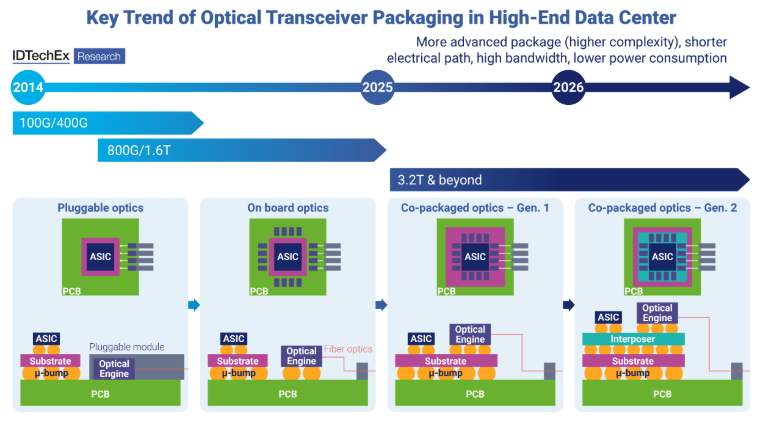
近年、光トランシーバ技術は、光学系を特定用途向け集積回路(ASIC)に近づける方向に着実にシフトしている。従来、スイッチのフロントパネルに挿入されるプラガブル・モジュールは、プリント回路基板の端に位置し、データセンターのスイッチとサーバーを接続する標準的なソリューションとして長い間利用されてきた。その柔軟性、交換の容易さ、簡単な拡張性から、依然として人気が高い。しかし、消費電力の増加や、フロントパネル面積あたりの帯域幅の制限など、課題も増えています。
このような制約に対処するため、業界は、電気信号に使用される銅トレースを短くする努力として、光エンジンをスイッチ ASIC の近くに移し始めている。このようなニアパッケージ・アプローチは電気的性能を向上させるが、それでも確立されたプラガブル・エコシステムから乖離しており、重要な制約が残っている。その結果、業界の多くは、光電コパッケージ技術のような完全統合ソリューションへの移行が直接進むと予想している。
IDTechExの調査レポート「光電コパッケージ技術(CPO) 2026-2036年:技術、市場、予測」は、この移行を詳細に調査している。CPO技術の最近の進歩をレビューし、新たなパッケージングアプローチを追跡し、主要企業の戦略を評価し、長期的な市場予測を示している。同レポートは、CPOの採用が今後10年でデータセンターのインフラをどのように再構築するかを明らかにしている。
ハイエンドデータセンターにおける光トランシーバの主要トレンド。出典:IDTechExIDTechEx
Co-Packaged Optics (CPO)における先進半導体パッケージング技術の重要性
従来のプラガブル光モジュールは、スイッチASICと光エンジンの間に長い電気トレースを必要とするため、信号損失、消費電力、レイテンシによる制約がますます大きくなっている。光電コパッケージ技術は、光エンジンをスイッチング・シリコンのずっと近くに配置することで、これらの制約を克服します。その成功は、スイッチASICやXPUへの光エンジンのシームレスな取り付けとともに、光ICと電子ICの高密度集積を可能にする高度な半導体パッケージング技術にかかっている。これには、2.5Dインターポーザ、TSV(Through Silicon Vias)、ファンアウト・ウェハレベル・パッケージング、最近ではハイブリッドボンディングによる3Dインテグレーションなど、さまざまなパッケージングアプローチが必要です。
GTC2025において、エヌビディアは2つの新しいネットワーキング・スイッチ・プラットフォーム、スペクトラムXフォトニクスと量子Xフォトニクスを発表した。これらのプラットフォームの中心となるのはTSMCのSoIC技術で、NVIDIAの設計に3D集積インフラを提供する。TSMCの先進的なバンプレス・ハイブリッド・ボンディング・プロセスであるSoIC Xバリアントは、ロジック・ダイやその他の異種コンポーネントを10マイクロメートル以下のピッチで垂直に積層することを可能にする。これにより、インターコネクト長が劇的に短縮され、抵抗とレイテンシが低減される。
ブロードコムを含む他の大手企業もTSMCのCOUPEプラットフォームを採用しており、CPOにおける3D集積とハイブリッドボンディングの重要性が高まっていることを裏付けている。
光電コパッケージ技術(CPO)市場の動向
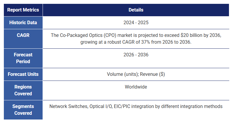
IDTechExによると、光電コパッケージ技術(CPO)市場は2036年までに200億米ドルを超え、2026年から2036年までの年平均成長率は37%と堅調に推移すると予測されている。CPOネットワークスイッチは、各スイッチが最大16個のCPO PICを内蔵する可能性があることから、売上高を独占すると見られている。AIシステム用光インタコネクトは、市場の約10%を占めると見られており、各AIアクセラレータは、通常1個の光インタコネクトPICを利用して、先端コンピューティングアプリケーションにおける高速データ処理と通信の需要増に対応している。
IDTechExの最新レポート「光電コパッケージ技術(CPO)2026-2036年:技術、市場、予測」は、コパッケージドオプティクス技術の最新の進歩を幅広く調査している。このレポートは、主要な技術革新とパッケージング動向を深く掘り下げ、バリューチェーン全体を包括的に分析している。業界主要企業の活動を徹底的に評価し、詳細な市場予測を行い、CPOの採用が将来のデータセンターアーキテクチャの景観をどのように再構築するかを予測している。
本レポートの中心は、先端半導体パッケージがコ・パッケージド・オプティクス技術の礎石であるという認識である。IDTechExは、様々な半導体パッケージング技術がCPOの領域で果たす可能性のある役割を理解することに重点を置いている。
本レポートの主な内容は以下の通りである:本レポートは、CPO(Co-Packaged Optics)の包括的な分析を提供し、様々な重要な側面を網羅している:
本レポートは、広範な調査と業界専門家へのインタビューに基づいており、データセンターとAI技術の未来を前進させるCo-Packaged Opticsの役割を戦略的に理解することに関心のあるすべての人に貴重な洞察を提供します。
市場予測-10年データセンター人口累積予測
目次1.エグゼクティブ・サマリー
1.1.最新の高性能AIデータセンターとはどのようなものか?
1.2.スイッチ:最新のデータセンターにおける主要コンポーネント
1.3.スイッチIC帯域幅の進歩とCPO(Co-Packaged Optics)技術の必要性
1.4.データセンター・アーキテクチャにおける主要課題の概要
1.5.ハイエンドデータセンターにおける光トランシーバの主要動向
1.6.プラグケーブルと比較した場合の CPO の設計判断
1.7.光エンジン(OE)とは
1.8.異種集積とCPO(Co-Packaged Optics)
1.9.半導体パッケージにおける相互接続技術の概要
1.10.主な CPO アプリケーション:ネットワークスイッチとコンピューティング光 I/O
1.11.高度な相互接続技術による EIC/PIC 統合
1.12. 2D から 3D への EIC/PIC 統合オプション
1.13.EIC/PICの各種パッケージング技術のベンチマーク表
1.14.3D光学エンジンとICのパッケージ例
1.15.CPO+XPU/スイッチASICの3種類のパッケージ構造
1.16.CPO技術の課題と将来性
1.17.サプライチェーンの概要
1.18.エヌビディア対ブロードコム:AIインフラとCPO技術における戦略的比較
1.19.CPO 製品のベンチマーク:エヌビディア対ブロードコム
1.20.エヌビディアとブロードコム:乖離する CPO エコシステム
1.21.現在のAIシステム・アーキテクチャ
1.22.IDTechExが予測する将来のAIアーキテクチャ(短期~中期)
1.23.IDTechExが予測する将来のAIアーキテクチャ(長期)
1.24.AIアクセラレーター市場の予測前回からの変更点
1.25.表による予測:サーバーボード、CPU、GPU/アクセラレータ
1.26.AIインターコネクト用光I/O CPO予測(出荷台数)
1.27.AIインターコネクト用光I/O CPO予測(売上高/市場規模)
1.28.AIアクセラレータ向けCPOネットワークスイッチ(L2スイッチ)の予測(出荷台数)
1.29.AIアクセラレータ向けCPOネットワークスイッチ(L2スイッチ)予測(市場規模・売上高)
1.30.CPO市場合計
1.31.EIC/PIC集積技術別CPO合計(出荷台数、百万台)
1.32.AIアクセラレータ用ネットワークスイッチ(L2スイッチ)のシステムインテグレーション パッケージング技術別予測(出荷台数)
1.33.光I/Oのシステムインテグレーション パッケージング技術別予測(出荷台数)
2.将来のAIシステムの課題と解決策
2.1.1.LLMの台頭と課題
2.1.2.最新の高性能AIデータセンターとはどのようなものか?
2.1.3.エヌビディアの最先端AIシステムに迫る
2.1.4.スイッチ:最新のデータセンターにおける主要コンポーネント
2.2.スケールアップ、スケールアウト、スケールアクロスネットワーク
2.2.1.スケールアップとスケールアウト
2.2.2.概要スケールアップ、スケールアウト、スケールクロス
2.3.ハイエンドデータセンター向けネットワークスイッチ・インターコネクトの課題
2.3.1.ハイエンドデータセンターにおけるネットワークスイッチの相互接続技術のロードマップ
2.3.2.広帯域システムにおけるセルデスのボトルネック
2.3.3.高帯域幅システムにおけるセルデスのボトルネックに対するソリューション
2.3.4.プラガブルオプティクス - ボトルネックは何か?
2.3.5.オンボードオプティクス(OBO)
2.3.6.コ・パッケージド・オプティクス(CPO)
2.3.7.プラガブル光トランシーバー接続における伝送損失
2.3.8.プラガブルオプティクスと CPO の比較
2.3.9.プラガブルと比較した CPO の設計上の決定事項
2.3.10.スイッチ IC の帯域幅の進歩と CPO 技術の必要性
2.3.11.L2 フロントサイドネットワークアーキテクチャ図 CPO と非 CPO
2.4.ハイエンドデータセンター向けコンピュートスイッチインターコネクト(光I/O)の課題
2.4.1.現在の AI システムのインターコネクトにおける銅線の数
2.4.2.AI における現在の銅線システムの限界
2.4.3.Nvidia のコネクティビティの選択:高帯域幅システムにおける銅と光の比較
2.4.4.高帯域幅システムにおける銅対光:ベンチマーク
2.4.5.ハイエンドAIシステムにおける銅から光への相互接続
2.4.6.現在のAIシステムアーキテクチャ
2.4.7.CuシステムによるL1バックサイド・コンピュート・アーキテクチャ
2.4.8.光インターコネクトによるL1バックサイド・コンピューティング・アーキテクチャ:Co-Packaged Optics (CPO)
2.4.9.銅線インターコネクトを光接続に交換する機会 - リーダーの発言は?
2.5.ハイエンドデータセンターにおける将来のAIシステム
2.5.1.電力効率の比較:CPO vs プラガブルオプティクス vs 銅インターコネクト
2.5.2.60cmデータ伝送技術ベンチマークのレイテンシー
2.5.3.IDTechEx が予測する将来の AI アーキテクチャ(短期~中期)
2.5.4.IDTechEx が予測する将来の AI アーキテクチャ(長期)
3. CO-PACKAGED OPTICS(CPO)入門
3.1.1.本章の内容
3.2.PICの主要概念
3.2.1.フォトニック集積回路(PIC)とは?
3.2.2.PICとシリコンフォトニクスの違い
3.2.3.PICのアーキテクチャ
3.2.4.PICの利点と課題
3.3.光エンジン(OE)
3.3.1.光エンジンとは?
3.3.2.光エンジンの仕組み
3.3.3.光電源
3.4.コ・パッケージド・オプティクス
3.4.1.コ・パッケージド・オプティクス(CPO)の3つの主要コンセプト
3.4.2.CPOの主要技術構成要素
3.4.3.CPOの利点:遅延
3.4.4.CPO の利点:消費電力
3.4.5.CPO の利点:データレート
3.4.6.CPOの価値提案の概要
3.4.7.CPOにおける今後の課題
4.CPOのパッケージング
4.1.1.光トランシーバーにパッケージされる主要コンポーネント
4.1.2.異種集積とコ・パッケージド・フォトニクス
4.1.3.ネットワークスイッチ用 CPO - パッケージングコンセプト
4.1.4.例:ネットワークスイッチ用1.6Tbpsコ・パッケージド・フォトニクス
4.1.5.XPU 用光 I/O としての CPO - パッケージングコンセプト
4.1.6.XPU用光I/OとしてのCPO-パッケージングコンセプト(続く)
4.1.7.例コンピュートシリコン用 CPO 統合
4.1.8.CPO パッケージング技術の概要
4.2.2.5Dおよび3D先端半導体パッケージング技術の概要と開発ロードマップ
4.2.1.半導体パッケージングの進化ロードマップ
4.2.2.半導体パッケージング - 技術の概要
4.2.3.先端半導体パッケージング性能の主要指標
4.2.4.半導体パッケージにおける相互接続技術の概要
4.2.5.2.5D パッケージング構造の概要
4.3. 2.5D Siベースのパッケージング技術
4.3.1. 2.Si を相互接続に用いる 5 次元パッケージ
4.3.2.貫通電極(TSV)の現状と将来
4.3.3.2.5次元Siベースパッケージングの開発動向
4.3.4.Si インターポーザーと Si ブリッジのベンチマーク
4.4. 2.5D 有機ベースパッケージング技術
4.4.1. 2.5D パッケージング - 高密度ファンアウト(FO)パッケージング
4.4.2.再配線層(RDL)
4.4.3.電子相互接続:SiO2対有機誘電体
4.4.4.2種類のファンアウト:パネルレベル
4.4.5.2種類のファンアウト:ウェハーレベル
4.4.6.ウェハレベルのファンアウトとパネルレベルのファンアウト:その違い
4.4.7.ファンアウト実装の主なトレンド
4.4.8.今後のファンアウトプロセスにおける課題
4.5. 2.5Dガラスベースのパッケージング技術
4.5.1.半導体パッケージにおけるガラスの役割
4.5.2.先端半導体パッケージのインターポーザーとしてのガラスコア
4.5.3.ガラスによるSiインターポーザーの限界の克服
4.5.4.ガラスと成形コンパウンドの比較
4.5.5.ガラスコア(インターポーザー)パッケージ - プロセスフロー
4.5.6.ガラスパッケージの課題
4.6.3D 先端半導体パッケージング技術
4.6.1.バンプ技術の進化
4.6.2.微細化バンプの課題
4.6.3. 先端半導体パッケージ用μバンプ
4.6.4.バンプレス Cu-Cu ハイブリッドボンディング
4.6.5.Cu-Cuハイブリッド接合の3つの方法:ベンチマーク
4.6.6.Cu-Cuハイブリッドボンディング製造プロセスの課題
4.7.CPO パッケージング:EIC と PIC の統合
4.7.1.EIC/PIC集積-従来型配線技術による
4.7.2.新しい配線技術によるEIC/PIC集積
4.7.3.2Dから3DへのEIC/PIC集積オプション
4.7.4.EIC/PIC の各種パッケージング技術のベンチマーク表
4.7.5.EIC/PICの2D集積の長所と短所
4.7.6.EIC/PICの2.5D統合の長所と短所
4.7.7.EIC/PICの3Dハイブリッド統合の長所と短所
4.7.8.EIC/PICの3Dモノリシック集積の長所と短所
4.8.EIC/PIC統合のためのTSV
4.8.1.CPOにおけるEIC/PIC統合用TSV
4.8.2.PIC と EIC の統合に TSV を使用する理由
4.8.3.シスコの光エンジンパッケージングアーキテクチャ
4.8.4.シスコ:EIC/PIC 統合用 2.5D チップオンチップ(CoC)パッケージングアーキテクチャ
4.8.5.シスコPIC/EIC 統合用 3D TSV
4.8.6.CPO における主な TSV 製造ステップと課題 - 1
4.8.7.CPOにおける主なTSV製造ステップと課題 - 2
4.8.8.シリコンフォトニクスのパッケージングオプション-TSVを使うか使わないか?
4.8.9.EIC/PIC集積用2.5D Siインターポーザーの長所と短所
4.9.EIC/PIC集積のためのファンアウト
4.9.1.ASEが提案するCPOパッケージ用ファンアウト・ソリューション
4.9.2.ASEのFOPOP-プロセス
4.9.3.CPO用FOPOPとWBパッケージの詳細分析
4.9.4.シリコンフォトニクス用光パッケージングプロセスの考察 - ASE
4.9.5.CPOにおけるPIC/EIC集積のためのSPILのFOEB(Fan-Out Embedded Bridge)構造
4.9.6.FOEB構造にPICとEICを集積するプロセスフロー
4.9.7.OE パッケージングにおけるプロセスの課題
4.9.8.ロックレー・フォトニクスはCPOパッケージング構造のためのFOWLPを提案している
4.9.9.ロックレーフォトニクスのFOWLP CPOパッケージングプロセスフロー-1
4.9.10.ロックレーフォトニクスのFOWLP CPOパッケージングプロセスフロー - 2
4.9.11.EIC/PIC統合のためのファンアウト使用の課題
4.10.ガラスベースのCPOパッケージング技術
4.10.1.コーニングのビジョン
4.10.2.ガラスベースCPOパッケージ光学部品 - パッケージング構造
4.10.3.ガラスベース Co-packaged optics - プロセス開発
4.10.4.コーニングの 102.4 Tb/s テストビークル
4.11.EIC/PIC 統合用ハイブリッドボンディング
4.11.1.TSMC:AI向け統合HPC技術プラットフォーム
4.11.2.TSMCの光エンジン・ロードマップ - 1
4.11.3.TSMCの光エンジン・ロードマップ - 2
4.11.4. TSMCの集積光インターコネクション・システム「iOIS」
4.11.5.EICとPICを3D SoICボンドで結合
4.11.6.ボンドピッチ微細化のロードマップ
4.12.OEとASIC/XPUなどのシステム統合
4.12.1.コ・パッケージングとコ・パッケージド・オプティクス(CPO)の比較
4.12.2.CPO+XPU/スイッチASICの3種類のパッケージ構造
4.12.3.光学エンジンと集積回路(IC)を2Dまたは2.5D構成でパッケージする例
4.12.4.2.5D構成におけるASICとのOE統合
4.12.5.光エンジンと集積回路(IC)を3D構成でパッケージングする例
4.12.6.将来の3D-CPO構造
4.12.7.NvidiaのSoC、HBM、EIC、PICのコ・パッケージ基板上への3D集積(TSVインターポーザ)
4.12.8.EIC/PIC の 3D 統合に基づく 51.2 Tb/s スイッチモジュールの例
4.12.9.ガラス・インターポーザー上でのEICとPICの3次元異種集積の製造プロセス
4.12.10.ガラスインターポーザー上にEIC/PICを3次元集積したスイッチモジュールの例
4.12.11.CPO技術の課題と将来の可能性
4.13.光アライメントとレーザー集積
4.13.1.CPOの作り方とボトルネック
4.13.2.カプラとFAUのインターフェース-CPOパッケージ成功の鍵
4.13.3.グレーティングとエッジカプラの比較シリコンフォトニクス用高密度光I/Oの課題
4.14.ファイバーアレイユニット(FAU)
4.14.1.光アライメントの課題と解決策 - 1
4.14.2.光アライメントの課題と解決策 - 2
4.14.3.光アライメントの課題と解決策 - 3
4.14.4.つのアライメント・アプローチ
4.14.5.光ファイバーパッケージの複雑さの軽減
4.14.6.主要な技術的課題:シリコン導波路とプレーナー光ファイバーとの間のサイズの不一致
4.14.7.ファイバーアレイユニット
4.14.8.ファイバー・アタッチ方法
4.14.9.CPO用FAUの主要プレーヤー
4.14.10.FOCI(ファイバーオプティカルコミュニケーション社)
4.14.11.FOCI の SiPh と CPO 製品ロードマップ
4.14.12.FOCIによるベースライン光ファイバ配列構造
4.14.13.光ファイバー配向構造のベンチマーク - 1
4.14.14.光ファイバー配向構造の変化のベンチマーク - 2
4.14.15.光ファイバー調心構造バリエーションベンチマーク - 3
4.14.16.センコーアドバンストコンポーネンツ
4.14.17.センコーアドバンストコンポーネンツ - 主要CPOソリューション
4.14.18.センコーアドバンストコンポーネンツ - パートナーシップ
4.14.19.CPOにおけるその他の光学部品サプライヤー(1)
4.14.20.CPOにおけるその他の光学部品サプライヤー(2)
4.15.レーザー集積化
4.15.1.オンチップ光源集積方式
4.15.2.CPO用外部レーザー(1)
4.15.3.CPO用外部レーザー(2)
4.15.4.レーザーアタッチ技術のベンチマーク - 1
4.15.5.レーザーアタッチ技術のベンチマーク - 2
4.15.6.異なるレーザー統合技術のベンチマーク
5.主要CPO企業:設計ロードマップ、戦略、エコシステム
5.1.サプライチェーンの概要
5.2.ブロードコム
5.3.ブロードコムの CPO 製品ベンチマーク
5.4.Broadcom の CPO 戦略
5.5.Broadcom の CPO 向け先進半導体パッケージング アプローチ
5.6.Broadcom の XPU-CPO
5.7.着脱式ファイバー コネクタ
5.8.Broadcom の CPO ロードマップ
5.9.ブロードコムの CPO エコシステム
5.10.エヌビディアCo-Packaged Optics の機会
5.11.エヌビディアの CPO 戦略
5.12.エヌビディアの CPO: Spectrum-X と Quantum-X
5.13.エヌビディアのCPO - パートナーシップ
5.14.エヌビディア:コ・パッケージド・オプティクスの課題と最終的な考察
5.15.エヌビディアとブロードコムの競争
5.16.エヌビディア対ブロードコム:AI インフラと CPO 技術における戦略的比較
5.17.CPO 製品のベンチマーク:エヌビディア対ブロードコム
5.18.エヌビディアとブロードコム:乖離する CPO エコシステム
5.19.マーベル
5.20.マーベルの XPU-CPO
5.21.マーベルのCPOリファレンス・デザイン
5.22.ラノバスの製品と進展 - (1)
5.23.ラノバスの製品と進捗状況 - (2)
5.24.ラノバス・パートナーシップ
5.25.メディアテック - CPO戦略/ロードマップ/パートナーシップ
5.26.ライトマター
5.27.ライトマター M1000
5.28.ライトマター - Passage ™:3Dフォトニックインターポーザ(1)
5.29.ライトマター - パサージュ™:3Dフォトニックインターポーザ(2)
5.30.ライトマターL シリーズ (3D CPO)
5.31.ライトマターパートナー
5.32.Ayar Labs TeraPHY
5.33.Ayar Labs AIスケールアップのための最近のコラボレーション - 1
5.34.Ayar Labs AIスケールアップのための最近のコラボレーション - 2
5.35.Cisco Co-Packaged Opticsのデモ
5.36.シスコCPOの電力効率
5.37.シスコ外部レーザー(ELFPP)
5.38.インテル光コンピュート・インターコネクト
5.39.Intel Optical Compute interconnect (2)
6.市場予測
6.1.AIアクセラレータ市場の予測:前回からの変更点
6.2.GPUとその他のアクセラレータの成長予測
6.3.表による予測:サーバーボード、CPU、GPU/アクセラレータ
6.4.AIインターコネクト用光I/O CPO予測(出荷台数)
6.5.AIインターコネクト用光I/O CPO予測(売上高/市場規模)
6.6.AIアクセラレータ向けCPOネットワークスイッチ(L2スイッチ)の予測(出荷台数)
6.7.AIアクセラレータ向けCPOネットワークスイッチ(L2スイッチ)データテーブル(出荷台数)
6.8.AIアクセラレータ向けCPOネットワークスイッチ(L2スイッチ)予測(市場規模・売上高)
6.9.CPO市場合計
6.10.EIC/PIC集積技術別CPO合計(出荷台数、百万台)
6.11.AIアクセラレータ用ネットワークスイッチ(L2スイッチ)のシステムインテグレーション パッケージング技術別予測(出荷台数)
6.12.光I/Oのシステム統合 パッケージング技術別予測 (出荷個数)
6.13.パッケージング技術別CPOユニット予測表
7.会社概要
7.1.ACCRETECH(研削工具)
7.2.AEPONYX
7.3.Amkor -アドバンスト・セミコンダクター・パッケージング
7.4.ASE -アドバンスト・セミコンダクター・パッケージング
7.5.Ayar Labs:AI アクセラレータインターコネクト
7.6.CEA-Leti (アドバンスト・セミコンダクター・パッケージング)
7.7.コヒーレントフォトニック集積回路ベースのトランシーバー
7.8.EFFECTフォトニクス
7.9.EVG(3Dハイブリッドボンディングツール)
7.10.グローバルファウンドリーズ
7.11.HDマイクロシステムズ
7.12.ヘンケル(半導体パッケージング、接着技術部門)
7.13.プログラマブルフォトニック集積回路
7.14.JCETグループ
7.15.JSR株式会社
7.16.ライトインテリジェンス
7.17.ライトマター
7.18.リオニクス
7.19.リパック
7.20.LPKF
7.21.三井金属鉱業(アドバンスト半導体パッケージング)
7.22.ナノワイヤード
7.23.レゾナック(RDL絶縁膜)
7.24.シンティル・フォトニクス
7.25.TOK
7.26.TSMC(アドバンスト・セミコンダクター・パッケージング)
7.27.Vitron (Through-Glass Via Manufacturing) -LPKF商標

SummaryCPO, optical interconnects, optical IO, data center, switches, AI, advanced semiconductor packaging, 2.5D, 3D, optical engine, EIC, PIC
The rise of Co-Packaged Optics (CPO)
In recent years, optical transceiver technology has been steadily shifting toward placing the optics closer to the Application-Specific Integrated Circuit (ASIC). Traditionally, pluggable modules inserted into the front panel of a switch sit at the edge of the printed circuit board and have long served as the standard solution for connecting switches and servers in data centers. They remain popular for their flexibility, ease of replacement, and straightforward scaling. However, they face growing challenges, especially rising power consumption and limits on how much bandwidth can be delivered per unit of front panel area.
To address these constraints, the industry has begun migrating the optical engine closer to the switch ASIC in an effort to shorten the copper trace used for electrical signalling. Although these near packaged approaches improve electrical performance, they still diverge from the well-established pluggable ecosystem and key limitations remain. As a result, many in the industry expect the transition to progress directly toward fully integrated solutions such as co packaged optics.
IDTechEx's report titled "Co-Packaged Optics (CPO) 2026 to 2036: Technologies, Market, and Forecasts" examines this transition in detail. It reviews recent advances in CPO technology, tracks emerging packaging approaches, assesses the strategies of leading companies, and provides long term market forecasts. The report highlights how CPO adoption is set to reshape data center infrastructure in the coming decade.
Key trend of optical transceivers in high-end data center. Source: IDTechEx
The importance of advanced semiconductor packaging technologies for Co-Packaged Optics (CPO)
Traditional pluggable optical modules are increasingly constrained by signal loss, power consumption, and latency because they require long electrical traces between the switch ASIC and the optical engine. Co-packaged optics overcomes these limitations by placing the optical engine much closer to the switching silicon. Its success depends on advanced semiconductor packaging technologies that enable high-density integration of photonic and electronic ICs, along with the seamless attachment of optical engines to switch ASICs or XPUs. This requires a range of packaging approaches, including 2.5D interposers, Through Silicon Vias (TSV), fan-out wafer-level packaging, and more recently, 3D integration supported by hybrid bonding.
At GTC 2025, NVIDIA introduced two new networking switch platforms, Spectrum X Photonics and Quantum X Photonics, both built on co packaged optics. Central to these platforms is TSMC's System on Integrated Chips technology, which provides the 3D integration infrastructure for NVIDIA's design. The SoIC X variant, TSMC's advanced bumpless hybrid bonding process, enables vertical stacking of logic dies and other heterogeneous components at sub ten micrometer pitch. This dramatically shortens interconnect length and reduces resistance and latency.
Other major players, including Broadcom, have also adopted TSMC's COUPE platform, underscoring the growing importance of 3D integration and hybrid bonding in CPO.
Co-Packaged Optics (CPO) Market trajectory
According to IDTechEx, the Co-Packaged Optics (CPO) market is projected to exceed US$20 billion by 2036, growing at a robust CAGR of 37% from 2026 to 2036. CPO network switches are expected to dominate revenue generation, driven by each switch potentially incorporating up to 16 CPO PICs. Optical interconnects for AI system will constitute approximately 10% of the market, with each AI accelerator typically utilizing one optical interconnect PIC to meet increasing demands for high-speed data processing and communication in advanced computing applications.
IDTechEx's latest report, titled "Co-Packaged Optics (CPO) 2026-2036: Technologies, Market, and Forecasts," offers an extensive exploration into the latest advancements within co-packaged optics technology. The report delves deep into key technical innovations and packaging trends, providing a comprehensive analysis of the entire value chain. It thoroughly evaluates the activities of major industry players and delivers detailed market forecasts, projecting how the adoption of CPO will reshape the landscape of future data center architecture.
Central to the report is the recognition of advanced semiconductor packaging as the cornerstone of co-packaged optics technology. IDTechEx places significant emphasis on understanding the potential roles that various semiconductor packaging technologies may play within the realm of CPO.
Key aspects of the report include:This report provides a comprehensive analysis of Co-Packaged Optics (CPO), encompassing various critical aspects:
The report is based on extensive research and interviews with industry experts and provides valuable insights for anyone interested in gaining a strategic understanding of Co-Packaged Optics' role in advancing the future of data center and AI technology.
Market Forecasts-10-year Data Center Population Cumulative Forecast
Table of Contents1. EXECUTIVE SUMMARY
1.1. What does a modern high-performance AI data center look like?
1.2. Switches: Key components in a modern data center
1.3. Advancements in Switch IC Bandwidth and the Need for Co-Packaged Optics (CPO) Technology
1.4. Overview of key challenges in data center architectures
1.5. Key trend of optical transceiver in high-end data centers
1.6. Design decisions for CPO compared to Pluggables
1.7. What is an Optical Engine (OE)
1.8. Heterogeneous integration and Co-Packaged Optics (CPO)
1.9. Overview of interconnection technique in semiconductor packaging
1.10. Key CPO applications: Network switch and computing optical I/O
1.11. EIC/PIC integration by advanced interconnect technique
1.12. 2D to 3D EIC/PIC integration options
1.13. Benchmark table of different packaging technologies for EIC/PIC
1.14. Examples of packaging a 3D optical engine with an IC
1.15. Three types of CPO + XPU/switch ASIC packaging structures
1.16. Challenges and future potential of CPO technology
1.17. Supply Chain Overview
1.18. NVIDIA vs Broadcom: Strategic Comparison in AI Infrastructure and CPO Technologies
1.19. CPO product benchmark: NVIDIA vs Broadcom
1.20. NVIDIA and Broadcom: Divergent CPO Ecosystems
1.21. Current AI system architecture
1.22. Future AI architecture (short to mid term) predicted by IDTechEx
1.23. Future AI architecture (long term) predicted by IDTechEx
1.24. Forecasting the AI accelerator Market: Changes From the previous Edition
1.25. Forecasts with table: Server boards, CPUs and GPUs/Accelerators
1.26. Optical I/O for AI interconnect CPO Forecast (units shipped)
1.27. Optical I/O for AI interconnect CPO Forecast (revenue/market size)
1.28. CPO network switches (L2 Switches) for AI accelerators forecast (units shipped)
1.29. CPO network switches (L2 Switches) for AI accelerators forecast (market size and revenue)
1.30. Total CPO market
1.31. Total CPO by different EIC/PIC integration technology (unit shipment, millions)
1.32. System integration of network switches (L2 Switches) for AI accelerators forecast by packaging technologies (unit shipped)
1.33. System integration of Optical I/O Forecast by packaging technologies (units shipped)
2. CHALLENGES AND SOLUTIONS FOR FUTURE AI SYSTEM
2.1.1. The rise and the challenges of LLM
2.1.2. What does a modern high-performance AI data center look like?
2.1.3. Closer look into NVIDIA's state-of-the-art AI system
2.1.4. Switches: Key components in modern data centers
2.2. Scale-up, Scale-out, and Scale-across network
2.2.1. Scale-up and Scale-Out
2.2.2. Overview: Scale-up, Scale-out, and Scale-across
2.3. Challenges in Network Switches Interconnect for High-end Data Centers
2.3.1. Roadmap of interconnect technology for network switches in high-end data centers
2.3.2. Serdes bottleneck in high-bandwidth systems
2.3.3. Solutions to Serdes bottlenecks in high-bandwidth systems
2.3.4. Pluggable optics - what are the bottlenecks?
2.3.5. On-Board Optics (OBO)
2.3.6. Co-Packaged Optics (CPO)
2.3.7. Transmission losses in a pluggable optical transceiver connection
2.3.8. Pluggable optics vs CPO
2.3.9. Design decisions for CPO compared to Pluggables
2.3.10. Advancements in switch IC bandwidth and the need for CPO technology
2.3.11. L2 frontside network architecture diagram CPO versus non-CPO
2.4. Challenges in Compute Switches Interconnect (i.e. Optical I/O) for High-end Data Centers
2.4.1. Number of Cu wires in current AI system Interconnects
2.4.2. Limitations in current copper systems in AI
2.4.3. Nvidia's connectivity choices: Copper vs optical for high-bandwidth systems
2.4.4. Copper vs. optical for high-bandwidth systems: Benchmark
2.4.5. Moving from Cu to optical interconnects for a high-end AI system
2.4.6. Current AI system architecture
2.4.7. L1 backside compute architecture with Cu systems
2.4.8. L1 backside compute architecture with optical interconnect: Co-Packaged Optics (CPO)
2.4.9. Opportunities for swapping copper interconnects to optical connects - what did the leader say?
2.5. Future AI system in high-end data center
2.5.1. Power efficiency comparison: CPO vs pluggable optics vs copper interconnects
2.5.2. Latency of 60cm data transmission technology benchmark
2.5.3. Future AI architecture (short to mid term) predicted by IDTechEx
2.5.4. Future AI architecture (long term) predicted by IDTechEx
3. INTRODUCTION TO CO-PACKAGED OPTICS (CPO)
3.1.1. What's covered in this chapter
3.2. PICs Key Concepts
3.2.1. What are Photonic Integrated Circuits (PICs)?
3.2.2. PICs vs Silicon Photonics - what are the differences
3.2.3. PIC architecture
3.2.4. Advantages and challenges of PIC
3.3. Optical Engine (OE)
3.3.1. What is an optical engine?
3.3.2. How an optical engine works
3.3.3. Optical power supplies
3.4. Co-Packaged Optics
3.4.1. Three key concepts in co-packaged optics (CPO)
3.4.2. Key technology building blocks for CPO
3.4.3. Benefits of CPO: Latency
3.4.4. Benefits of CPO: Power consumption
3.4.5. Benefits of CPO: Data rate
3.4.6. Overview of value proposition of CPO
3.4.7. Future challenges in CPO
4. PACKAGING FOR CO-PACKAGED OPTICS (CPO)
4.1.1. Key components to be packaged in an optical transceiver
4.1.2. Heterogeneous integration and Co-Packaged Photonics
4.1.3. CPO for network switch - packaging concept
4.1.4. Example: 1.6 Tbps Co-packaged optics for network switch
4.1.5. CPO as optical I/O for XPUs - packaging concept
4.1.6. CPO as optical I/O for XPUs - packaging concept (follow)
4.1.7. Example: CPO integration for compute silicon
4.1.8. Overview of CPO packaging technologies
4.2. Overview and development roadmap of 2.5D and 3D advanced semiconductor packaging technologies
4.2.1. Evolution roadmap of semiconductor packaging
4.2.2. Semiconductor packaging - an overview of technology
4.2.3. Key metrics for advanced semiconductor packaging performance
4.2.4. Overview of interconnection technique in semiconductor packaging
4.2.5. Overview of 2.5D packaging structure
4.3. 2.5D Si-based Packaging Technologies
4.3.1. 2.5D packaging that involves Si as interconnect
4.3.2. Through Si Via (TSV) - now and the future
4.3.3. Developing trend for 2.5D Si-based packaging
4.3.4. Si interposer vs Si bridge benchmark
4.4. 2.5D Organic-based Packaging technologies
4.4.1. 2.5D packaging - high density fan-out (FO) packaging
4.4.2. Redistribution Layer (RDL)
4.4.3. Electronic interconnects: SiO2 vs organic dielectric
4.4.4. Two types of fan-out: Panel level
4.4.5. Two types of fan-out: Wafer level
4.4.6. Wafer level fan-out vs panel level fan-out: The differences
4.4.7. Key trends in fan-out packaging
4.4.8. Challenges in future fan-out process
4.5. 2.5D Glass-based Packaging Technologies
4.5.1. Roles of glass in semiconductor packaging
4.5.2. Glass core as interposer for advanced semiconductor packaging
4.5.3. Overcoming limitations of Si interposers with glass
4.5.4. Glass vs molding compound
4.5.5. Glass core (interposer) package - process flow
4.5.6. Challenges of glass packaging
4.6. 3D Advanced Semiconductor Packaging Technologies
4.6.1. Evolution of bumping technologies
4.6.2. Challenges in scaling bumps
4.6.3. µ bump for advanced semiconductor packaging
4.6.4. Bumpless Cu-Cu hybrid bonding
4.6.5. Three ways of Cu-Cu hybrid bonding: Benchmark
4.6.6. Challenges in Cu-Cu hybrid bonding manufacturing process
4.7. CPO Packaging: EIC and PIC Integration
4.7.1. EIC/PIC integration - by conventional interconnect technique
4.7.2. EIC/PIC integration by emerging interconnect technique
4.7.3. 2D to 3D EIC/PIC integration options
4.7.4. Benchmark table of different packaging technologies for EIC/PIC
4.7.5. Pros and Cons of 2D integration of EIC/PIC
4.7.6. Pros and Cons of 2.5D integration of EIC/PIC
4.7.7. Pros and Cons of 3D hybrid integration of EIC/PIC
4.7.8. Pros and Cons of 3D monolithic integration of EIC/PIC
4.8. TSV for EIC/PIC Integration
4.8.1. TSV for EIC/PIC integration in CPO
4.8.2. Why using TSV for PIC and EIC integration
4.8.3. Cisco packaging architectures of optical engine over generations
4.8.4. Cisco: 2.5D Chip-on-Chip (CoC) packaging architecture for EIC/PIC integration
4.8.5. Cisco: 3D TSV for PIC/EIC integration
4.8.6. Key TSV Fabrication steps and challenges in CPO - 1
4.8.7. Key TSV fabrication steps and challenges in CPO - 2
4.8.8. Packaging options for silicon photonics - w/ or w/o TSV?
4.8.9. Pros and Cons of 2.5D Si interposer for EIC/PIC integration
4.9. Fan-out for EIC/PIC Integration
4.9.1. ASE's proposed fan-out solution for CPO packaging
4.9.2. FOPOP from ASE - process
4.9.3. Detailed analysis of FOPOP vs WB packaging for CPO
4.9.4. Optical packaging process considerations for silicon photonics - ASE
4.9.5. SPIL's Fan-Out Embedded Bridge (FOEB) structure for PIC/EIC integration in CPO
4.9.6. Process flow of integrating PIC and EIC in a FOEB structure
4.9.7. Process challenges in packaging OE
4.9.8. Rockley Photonics proposes FOWLP for CPO packaging structure
4.9.9. Rockley Photonics' FOWLP CPO packaging process flow - 1
4.9.10. Rockley Photonics' FOWLP CPO packaging process flow - 2
4.9.11. Challenges of using fan-out for EIC/PIC integration
4.10. Glass-based CPO Packaging Technologies
4.10.1. Glass-based Co-packaged optics - Corning's vision
4.10.2. Glass-based Co-packaged optics - packaging structure
4.10.3. Glass-based Co-packaged optics - process development
4.10.4. Corning's 102.4 Tb/s test vehicle
4.11. Hybrid bonding for EIC/PIC integration
4.11.1. TSMC: Integrated HPC technology platform for AI
4.11.2. Optical engine roadmap from TSMC - 1
4.11.3. Optical engine roadmap from TSMC - 2
4.11.4. iOIS - Integrated Optical Interconnection System from TSMC
4.11.5. Combining EIC and PIC with 3D SoIC bond
4.11.6. Roadmap of bond pitch scaling
4.12. System integration of OE and ASIC/XPU, etc
4.12.1. Co-Packaging vs Co-Packaged Optics (CPO)
4.12.2. Three types of CPO + XPU/switch ASIC packaging structures
4.12.3. Examples of packaging an optical engine with an integrated circuit (IC) in a 2D or 2.5D configuration
4.12.4. OE integration with ASIC in a 2.5D configuration
4.12.5. Examples of packaging an optical engine with an integrated circuit (IC) in a 3D configuration
4.12.6. Future 3D-CPO structure
4.12.7. Nvidia's 3D integration of SoC, HBM, EIC and PIC on co-packaged substrates (TSV interposer)
4.12.8. Example of a 51.2 Tb/s switch module based on 3D integration of EIC/PIC
4.12.9. Process in fabrication of the 3D heterogeneous integration of EIC and PIC on a glass interposer
4.12.10. Example of a switch module based on 3D integration of EIC/PIC on glass interposer
4.12.11. Challenges and Future Potential of CPO Technology
4.13. Optical alignment and Laser Integration
4.13.1. How CPO is Built and the Bottleneck
4.13.2. Interface between Coupler and FAU - Key to the success of CPO packaging
4.13.3. Grating vs Edge Couplers: Challenges in high-density optical I/O for silicon photonics
4.14. Fiber Array Unit (FAU)
4.14.1. Optical alignment challenges and solutions - 1
4.14.2. Optical alignment challenges and solutions - 2
4.14.3. Optical alignment challenges and solutions - 3
4.14.4. Two alignment approaches
4.14.5. Reducing optical fiber packaging complexity
4.14.6. Key technical challenge: The size mismatch between silicon waveguides and planar optical fibers
4.14.7. Fiber Array Unit
4.14.8. Fiber Attach Methods
4.14.9. Key players in FAU for CPO
4.14.10. FOCI (Fiber Optical Communication Inc.)
4.14.11. FOCI's SiPh and CPO product roadmap
4.14.12. Baseline Optical Fiber Alignment Structure from FOCI
4.14.13. Benchmark of Optical Fiber Alignment Structure Variations - 1
4.14.14. Benchmark of Optical Fiber Alignment Structure Variations - 2
4.14.15. Benchmark of Optical Fiber Alignment Structure Variations - 3
4.14.16. Senko Advanced Components
4.14.17. Senko Advanced Components - Key CPO solution
4.14.18. Senko Advanced Components - Partnership
4.14.19. Suppliers of Other Optical Components in CPO (1)
4.14.20. Suppliers of Other Optical Components in CPO (2)
4.15. Laser Integration
4.15.1. On-chip light source integration methods
4.15.2. External lasers for CPO (1)
4.15.3. External lasers for CPO (2)
4.15.4. Laser attach technology benchmark - 1
4.15.5. Laser attach technology benchmark - 2
4.15.6. Benchmark of different laser integration technology
5. KEY CPO COMPANIES: DESIGN ROADMAP, STRATEGIES, ECOSYSTEM
5.1. Supply Chain Overview
5.2. Broadcom
5.3. Broadcom CPO Products Benchmark
5.4. Broadcom's CPO strategy
5.5. Advanced Semiconductor Packaging Approach for Broadcom's CPO
5.6. Broadcom's XPU-CPO
5.7. Detachable fiber connector
5.8. Broadcom's CPO roadmap
5.9. Broadcom CPO ecosystem
5.10. Nvidia: Opportunities for Co-Packaged Optics
5.11. Nvidia's CPO strategy
5.12. NVIDIA'S CPO: Spectrum-X and Quantum-X
5.13. NVIDIA'S CPO - Partnerships
5.14. Nvidia: Challenges and final thoughts for Co-Packaged Optics
5.15. Competition between Nvidia and Broadcom
5.16. NVIDIA vs Broadcom: Strategic Comparison in AI Infrastructure and CPO Technologies
5.17. CPO product benchmark: NVIDIA vs Broadcom
5.18. NVIDIA and Broadcom: Divergent CPO Ecosystems
5.19. Marvell
5.20. Marvell's XPU-CPO
5.21. Marvell's CPO reference design
5.22. Ranovus products and progress - (1)
5.23. Ranovus products and progress - (2)
5.24. Ranovus Partnerships
5.25. MediaTek - CPO strategy/Roadmap/Partnership
5.26. Lightmatter
5.27. Lightmatter M1000
5.28. Lightmatter - Passage ™: 3D Photonic Interposer (1)
5.29. Lightmatter - Passage ™: 3D Photonic Interposer (2)
5.30. Lightmatter: L-Series (3D CPO)
5.31. Lightmatter: Partners
5.32. Ayar Labs TeraPHY
5.33. Ayar Labs Recent Collaboration for AI scale-up - 1
5.34. Ayar Labs Recent Collaboration for AI scale-up - 2
5.35. Cisco Co-Packaged Optics demo
5.36. Cisco: CPO power efficiency
5.37. Cisco: External lasers (ELFPP)
5.38. Intel Optical Compute interconnect
5.39. Intel Optical Compute interconnect (2)
6. MARKET FORECASTS
6.1. Forecasting the AI accelerator Market: Changes From the previous Edition
6.2. Forecasting Growth in GPUs and Other Accelerators
6.3. Forecasts with table: Server boards, CPUs and GPUs/Accelerators
6.4. Optical I/O for AI interconnect CPO Forecast (units shipped)
6.5. Optical I/O for AI interconnect CPO Forecast (revenue/market size)
6.6. CPO network switches (L2 Switches) for AI accelerators forecast (units shipped)
6.7. CPO network switches (L2 Switches) for AI accelerators data table (units shipped)
6.8. CPO network switches (L2 Switches) for AI accelerators forecast (market size and revenue)
6.9. Total CPO market
6.10. Total CPO by different EIC/PIC integration technology (unit shipment, millions)
6.11. System integration of network switches (L2 Switches) for AI accelerators forecast by packaging technologies (unit shipped)
6.12. System integration of Optical I/O Forecast by packaging technologies (units shipped)
6.13. Table for CPO unit forecast by packaging technologies
7. COMPANY PROFILES
7.1. ACCRETECH (Grinding Tool)
7.2. AEPONYX
7.3. Amkor — Advanced Semiconductor Packaging
7.4. ASE — Advanced Semiconductor Packaging
7.5. Ayar Labs: AI Accelerator Interconnect
7.6. CEA-Leti (Advanced Semiconductor Packaging)
7.7. Coherent: Photonic Integrated Circuit-Based Transceivers
7.8. EFFECT Photonics
7.9. EVG (3D Hybrid Bonding Tool)
7.10. GlobalFoundries
7.11. HD Microsystems
7.12. Henkel (Semiconductor packaging, Adhesive Technologies division)
7.13. iPronics: Programmable Photonic Integrated Circuits
7.14. JCET Group
7.15. JSR Corporation
7.16. Lightelligence
7.17. Lightmatter
7.18. LioniX
7.19. LIPAC
7.20. LPKF
7.21. Mitsui Mining & Smelting (Advanced Semiconductor Packaging)
7.22. NanoWired
7.23. Resonac (RDL Insulation Layer)
7.24. Scintil Photonics
7.25. TOK
7.26. TSMC (Advanced Semiconductor Packaging)
7.27. Vitron (Through-Glass Via Manufacturing) — A LPKF Trademark
ご注文は、お電話またはWEBから承ります。お見積もりの作成もお気軽にご相談ください。本レポートと同分野(光通信)の最新刊レポート
IDTechEx社の フォトニクス - Photonics分野 での最新刊レポート
よくあるご質問IDTechEx社はどのような調査会社ですか?IDTechExはセンサ技術や3D印刷、電気自動車などの先端技術・材料市場を対象に広範かつ詳細な調査を行っています。データリソースはIDTechExの調査レポートおよび委託調査(個別調査)を取り扱う日... もっと見る 調査レポートの納品までの日数はどの程度ですか?在庫のあるものは速納となりますが、平均的には 3-4日と見て下さい。
注文の手続きはどのようになっていますか?1)お客様からの御問い合わせをいただきます。
お支払方法の方法はどのようになっていますか?納品と同時にデータリソース社よりお客様へ請求書(必要に応じて納品書も)を発送いたします。
データリソース社はどのような会社ですか?当社は、世界各国の主要調査会社・レポート出版社と提携し、世界各国の市場調査レポートや技術動向レポートなどを日本国内の企業・公官庁及び教育研究機関に提供しております。
|
|