量子技術向け材料 2026-2046年:市場、動向、プレーヤー、予測Materials for Quantum Technologies 2026-2046: Market, Trends, Players, Forecasts 量子コンピューティング、量子センシング、量子通信における材料機会の20年予測。量子応用のための超伝導体、フォトニクス、PIC、ナノ材料、ダイヤモンドの技術、主要プレーヤー、サプライチェーンダイナミク... もっと見る

サマリー
量子コンピューティング、量子センシング、量子通信における材料機会の20年予測。量子応用のための超伝導体、フォトニクス、PIC、ナノ材料、ダイヤモンドの技術、主要プレーヤー、サプライチェーンダイナミクス。
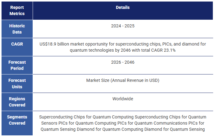
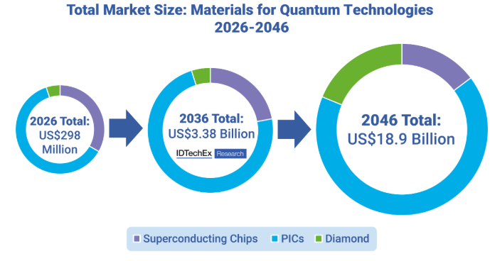
量子技術は現在最も急成長しているディープテック市場の一つであるが、その性能と拡張性は材料、部品、製造プロセスにおける課題によってしばしば阻まれている。本レポートでは、量子コンピューティング、量子センシング、量子通信向けの材料におけるビジネスチャンスと新たなソリューションを分析しており、量子技術向けの超伝導チップ、PIC、ダイヤモンドの市場機会は、2036年までに33億8000万米ドル、2046年までに 189億米ドルに達すると予測され、全予測期間の年平均成長率は23.1%である。
量子テクノロジー産業は多様性に富んでおり、製品、ビジネスモデル、そして大学のスピンアウトから政府、国際企業まで幅広いプレーヤーがグローバルに分布している。しかし、IDTechExが見出したのは、業界全体を通じて、量子技術のスケーラビリティ、ひいては商業的実現性を可能にする主要な材料プラットフォームにチャンスがあるということである。このような材料プラットフォームは、製品の「量子的優位性」を引き出すために活用される量子システムの物理的基盤である。量子コンピューターで古典的な難問の計算を可能にしたり、量子センサーで桁違いに高い感度を実現したり、量子通信で根本的に安全な暗号ソリューションを生み出したりするためである。
出典IDTechExリサーチ
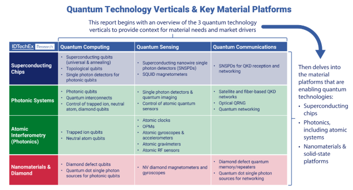
3つの量子市場、3つの主要材料プラットフォーム
量子技術は通常、量子コンピューティング、 量子センシング、量子通信の3つの中核製品に分類される。この分類は通常、政府および民間の量子戦略で使用されており、IDTechExは各分野の詳細な分析を含む個別の市場調査レポートを発行している。
しかし、材料の観点からは、量子技術を物理的な「プラットフォーム」や量子システムによって分類する方が有益である。このアプローチでは、アプリケーションではなく、各製品に共通する材料やコンポーネントによって、各製品間の接点を浮き彫りにすることができる。
量子技術にとって最も重要な3つの材料プラットフォームは、以下のように分類できる。
出典IDTechEx Research.
量子テクノロジーにおけるフォトニクスの可能性
フォトニクスはすでに古典的な情報技術に革命を起こしており、フォトニック集積回路(PIC)をベースとしたトランシーバーは、AIデータセンター内で前例のない規模の高速通信を可能にしている。量子テクノロジーにとって、PICは、これまでラボベースのセットアップで光学テーブル全体を占めていた光学系をチップスケールまで縮小できる可能性を持っている。
しかし、量子PICの要件は他のアプリケーションとは大きく異なる。量子システムは壊れやすいため、量子PICは損失に対する耐性が非常に低く、ダイヤモンドの原子や点欠陥のようなシステムに対応するためには、従来の電気通信やデータ通信業界では馴染みのない波長で動作する必要もある。
このような要求に対応するため、フォトニクスのイノベーターたちはシリコン以外のPIC材料プラットフォームを模索しており、その一例として窒化シリコン(SiN)、薄膜ニオブ酸リチウム(TFLN)、チタン酸バリウム(BTO)などが量子フォトニクス業界の新星として挙げられる。これらの材料のチャンピオンは、PsiQuantum、QuiX Quantum、Quantum Computing Inc (QCi)などの量子業界内からも、外部のファウンドリーやパートナーからも生まれている。
本レポートでは、量子チップの材料、製造プロセス、パッケージング傾向、テスト、さらに人工ダイヤモンドやナノ材料の新たなビジネスチャンスについて取り上げている。
本レポートの主要な側面
本レポートは、量子技術産業における材料機会の詳細な検証を目的としており、超伝導体、フォトニクス、ナノ材料にわたる技術革新、市場勢力、サプライチェーンダイナミクスに焦点を当てています。
主要な側面
本レポートは、以下のトピックをすべて網羅しています。
量子技術に対する材料要件の分析
20年間のきめ細かな市場規模予測
目次1.要旨
1.1.アナリストの見解 - 量子技術向け材料
1.2.量子テクノロジー市場の概要
1.3.レポートの動機量子技術向け材料
1.4.レポートの概要 - 量子技術分野と材料プラットフォーム
1.5.量子コンピューティングにおける材料の役割の概要
1.6.量子コンピューティングにおける材料機会の概要
1.7.量子センシング材料の概要
1.8.量子センシングにおけるコンポーネントのロードマップ
1.9.量子ネットワーキングと量子通信における材料の可能性
1.10.量子テクノロジーにおける超伝導体
1.11.量子技術における超伝導材料の選択において重要な役割を果たす臨界温度
1.12.超伝導量子チップの製造プロセスの概要
1.13.超伝導チップの製造:SQUID vs 量子コンピューティングチップ
1.14.KIDとTESが研究段階にある一方で、SNSPDはどのように普及したのか?
1.15.量子技術における超伝導体の重要な要点
1.16.なぜフォトニクスは量子技術に有用なのか?
1.17.量子技術におけるフォトニクス、シリコンフォトニクス、光学の概要
1.18.量子技術におけるPICの役割
1.19.量子技術開発者によるフォトニクス企業買収の急増
1.20.量子通信とネットワーキングにおけるシリコンフォトニクスプラットフォームのビジネスチャンス
1.21.量子技術用フォトニックパッケージングの動向 - オルターテクノロジー
1.22.量子PIC材料プラットフォームのベンチマーク
1.23.量子アプリケーション用PICの結論
1.24.量子応用におけるナノ材料とダイヤモンドの初期段階の使用例
1.25.量子技術におけるダイヤモンドの概要
1.26.本レポートの予測線とその構成
1.27.予測結果の概要
1.28.量子技術向け超電導チップの市場規模予測 2026-2046年
1.29.量子テクノロジー向けPICの市場規模予測 2026-2046年
1.30.量子テクノロジー向けダイヤモンドの市場規模予測 2026-2046年
2.序論
2.1.量子テクノロジー市場の概要
2.2.レポートの動機量子技術向け材料
2.3.量子技術向け材料プラットフォーム
2.4.レポートの概要 - 量子技術分野と材料プラットフォーム
2.5.レポートの構成
3.量子技術市場
3.1.量子コンピューティング市場概要
3.1.1.量子コンピューティング市場概観
3.1.2.量子コンピュータの紹介
3.1.3.量子エコシステムは成長し、様々なアプローチをカバーしている
3.1.4.主要な量子ハードウェアの将来性と課題をまとめる
3.1.5.代替量子ハードウェアの将来性と課題
3.1.6.量子至上主義と量子ビット数
3.1.7.コヒーレンス時間の比較
3.1.8.量子ビットの忠実度とエラー率
3.1.9.量子ビットへのノイズ効果
3.1.10.その他の情報は、IDTechEx の市場調査レポート「量子コンピューティング市場 2026-2046年:技術、動向、プレイヤー、予測」に記載されている
3.2.量子コンピューティング用材料
3.2.1.量子コンピューティングにおける材料の役割の概要
3.2.2.量子コンピューティングのためのハードウェアに依存しないインフラ・プラットフォームは、既存技術の新市場となる
3.2.3.材料の欠陥はノイズの主要な原因である
3.2.4.量子コンピューティングにおける材料機会の概要
3.3.量子センシング:市場概要
3.3.1.量子センサー市場概観
3.3.2.量子センサーとは何か?
3.3.3.量子センサーの価値提案はハードウェアアプローチ、アプリケーション、競合によって異なる
3.3.4.IDTechExの市場調査で対象となる量子センサー技術
3.3.5.量子センサーの主要産業
3.3.6.量子センサーの主要技術プラットフォーム
3.3.7.追加情報はIDTechExの市場調査レポート「量子センサー市場 2026-2046年:技術、動向、プレーヤー、予測」に掲載されている
3.4.量子センシング用材料
3.4.1.量子センシング用材料の概要
3.4.2.原子およびダイヤモンドベースの量子センシング用特殊コンポーネント
3.4.3.量子センシング用部材の主要企業
3.4.4.量子センシング用コンポーネントのロードマップ
3.4.5.量子センシング用コンポーネントのロードマップとその応用
3.4.6.量子ファウンドリー」の設立は、チップスケールの量子センサー用小型部品の製造規模を拡大する鍵
3.5.量子通信:市場の概要
3.5.1.量子通信市場の「概観」
3.5.2.データ・セキュリティに対する量子の脅威
3.5.3. 「Hack Now Decrypt Later」(HNDL)とQ-Day/Y2Qへの準備
3.5.4.データ・セキュリティに対する量子のソリューション
3.5.5.光QRNG技術の動作原理
3.5.6.QRNG の既存技術に対する主な価値提案とは?
3.5.7.QRNG 製品を開発する主要企業(ハードウェアアプローチ別に分類)
3.5.8.量子乱数生成器(QRNG)のアプリケーション
3.5.9.なぜQKDは他の鍵交換メカニズムよりも安全なのか?
3.5.10.QKD技術を開発する主要プレイヤーの概要(1)
3.5.11.QKD技術を開発する主なプレイヤーの概要(2)
3.5.12.量子ネットワークとは?
3.5.13.両商業戦略としての量子ネットワーク構築 - シスコ
3.5.14.その他の情報はIDTechExの市場調査レポート「量子通信市場2024-2034年:技術、動向、プレーヤー、予測」
3.6.量子通信の材料
3.6.1.QRNG デバイスの主なフォームファクターアプローチは?
3.6.2.光QRNGデバイスの構成要素
3.6.3.QKDシステムの基本原理と構成要素
3.6.4.信頼できるノードと信頼できるリレーの役割
3.6.5.エンタングルメント・スワッピングと光スイッチ
3.6.6.チップスケール QKD への取り組みは PIC 産業の成長から恩恵を受ける
3.6.7.量子ネットワーキングと量子通信における材料の可能性
4.超伝導体
4.1.量子技術のための超伝導材料
4.1.1.章の概要量子テクノロジーにおける超伝導体
4.1.2.量子テクノロジーにおける超伝導体の応用
4.1.3.量子技術における超電導材料選択において重要な役割を果たす臨界温度
4.1.4.超電導材料のサプライチェーンにおける重要な検討事項
4.1.5.量子技術における超電導バリューチェーンの概要
4.1.6.室温超伝導体 - 量子技術市場を必ずしも解き放たない理由
4.2.超伝導量子回路:作製、パッケージング、テスト
4.2.1.超伝導量子ビットの紹介:動機と概要
4.2.2.超伝導量子ビット入門:動機と概要
4.2.2:非調和振動子と「トランスモン」量子ビット
4.2.3.トランスモン超伝導量子ビット:構造、材料、作製
4.2.4.工業プロセスによる超伝導量子ビットの製造
4.2.5.超伝導量子回路の欠陥とノイズ源
4.2.6.超伝導量子ビットの製造における品質とスケーラビリティのトレードオフ
4.2.7.超伝導量子ビットのコヒーレンス時間の延長は、製造方法とパッケージング方法の改善によって達成される
4.2.8.超伝導チップのスルーシリコン・ビアとフリップチップ・ボンディング
4.2.9.現在の回路アーキテクチャとパッケージングによるスケーラビリティの限界
4.2.10.スケーラビリティの限界を解決する3Dパッケージングとチップレット - QuantWare
4.2.11.量子コンピューティングのためのチップレットアーキテクチャ - Rigetti
4.2.12.量子回路用超伝導キャップ - リゲッティ
4.2.13.量子チップテスト入門
4.2.14.量子チップでは何をテストする必要があるのか?
4.2.15.自動量子チップ試験システム - Orange Quantum Systems
4.2.16.超伝導量子チップの製造プロセスのまとめ
4.3.超伝導量子干渉素子(SQUID)
4.3.1.SQUIDの動作原理
4.3.2.SQUID 製造サービスは専門ファウンドリーが提供
4.3.3.SQUID の応用
4.3.4.SQUIDの商業的応用と市場機会
4.3.5.超伝導チップの製造:SQUID vs 量子コンピューティングチップ
4.3.6.SWOT分析:超伝導量子干渉素子(SQUID)
4.4.超伝導ナノワイヤー単一光子検出器(SNSPD)
4.4.1.超伝導ナノワイヤー単一光子検出器(SNSPD)
4.4.2.量子コンピューティングと量子通信のコンポーネントとしての SNSPD
4.4.3.超伝導材料の進歩がSNSPD開発を牽引
4.4.4.フォトニック量子コンピューティングチップセット PsiQuantum における SNSPD
4.4.5.SNSPD アレイをキロピクセル以上に拡大する研究 - NIST
4.4.6.SNSPD と SNSPD アレイの作製
4.4.7.商用SNSPDプレーヤーの比較
4.4.8.SWOT分析:超伝導ナノワイヤー単一光子検出器(SNSPD)
4.5.運動インダクタンス検出器(KID)と遷移端センサー(TES)
4.5.1.運動インダクタンス検出器(KID)
4.5.2.トランジション・エッジ・センサ(TES)
4.5.3.KIDやTESが研究途上にある一方で、SNSPDはどのように普及したのか?
4.5.4.単一光子検出器技術の比較
4.6.章まとめ:量子技術における超伝導体
4.6.1.量子テクノロジーにおける超伝導体の用途
4.6.2.量子技術における超伝導体のキーポイント
5.フォトニクス
5.1.量子技術におけるフォトニクス、シリコンフォトニクス、光学の概要
5.1.1.なぜフォトニクスが量子技術に有用なのか?
5.1.2.章の概要量子テクノロジーにおけるフォトニクス
5.2.量子技術のためのフォトニック集積回路(PIC)入門
5.2.1.フォトニック集積回路(PIC)とは?
5.2.2.フォトニック集積回路の一般的な利点と課題
5.2.3.PICの集積化スキーム
5.2.4.量子技術におけるPICの役割
5.2.5.フォトニック集積回路と光テーブルや固定光学系との比較
5.2.6.量子技術におけるフォトニック集積回路の利点
5.2.7.量子技術開発企業によるフォトニクス企業の買収急増
5.2.8.光学材料の動作周波数窓
5.2.9.量子PIC材料プラットフォームのベンチマーク
5.2.10.SiN、TFLN、BTO ファウンドリ
5.2.11.量子PICの材料プラットフォームは?
5.2.12.SPIE Photonics Westから見た量子産業における将来のPIC要件
5.2.13.量子技術におけるフォトニック集積回路の概要
5.3.フォトニック量子コンピューティングのためのフォトニック集積回路(PIC)
5.3.1.量子コンピューティング用フォトニックプラットフォームの概要
5.3.2.フォトニック量子コンピューターの初期化、操作、読み出し
5.3.3.SiNフォトニック量子プロセッサの商用化 - QuiX Quantum
5.3.4.量子コンピュータ用フォトニックチップセット - PsiQuantum
5.3.5.フォトニック量子コンピューティングに必要な単一光子検出器、電気光学材料、標準シリコンの代替品 - PsiQuantum
5.3.6.量子PICに関するCEA Letiの目標
5.3.7.量子フォトニックビルディングブロック - imec
5.3.8.量子PICに潜在的な関心を持つ新しいTFLNファウンドリ
5.3.9.SWOT分析:フォトニック量子コンピューティング用PIC
5.4.トラップドイオン・中性原子量子コンピューティング用フォトニック集積回路(PIC)
5.4.1.トラップイオン及び中性原子量子コンピュータの紹介
5.4.2.捕捉イオン量子コンピュータの初期化、操作、読み出し
5.4.3.完全集積型捕捉イオンチップのための材料の課題
5.4.4.捕捉型イオン量子コンピューターのためのPIC
5.4.5.トラップドイオン量子コンピューターのリーダーがインフィニオンと提携
5.4.6.SiNQ: 量子関連 33 波長用の窒化シリコン PDK - Wave Photonics
5.4.7.中性原子量子コンピューターの初期化、操作、読み出し
5.4.8.中性原子量子コンピュータ用PIC - Pasqal社がAEPONYX社を買収
5.4.9.中性原子量子ビットの高速量子制御のためのAlN圧電アクチュエータ付きSiN導波路 - QuEra
5.4.10.原子時計、RFセンサー、量子コンピューターの実用化の中心にPIC - Infleqtion (1/2)
5.4.11.原子センシングとコンピューティングのためのフォトニック材料 - Infleqtion (2/2)
5.4.12.SWOT分析:SWOT分析:捕捉イオンと中性原子量子コンピューティングのためのPIC
5.5.量子ネットワークのためのフォトニクスと量子通信
5.5.1.資源としてのエンタングルメント
5.5.2.量子ネットワークのためのその他のコンポーネント周波数変換とスイッチ
5.5.3.光ファイバーや量子インターコネクト材料の改良の機会
5.5.4.量子ネットワーク用エンタングル光子源 - ルミノ・テクノロジーズ
5.5.5.量子通信用の新しいGaAs単一光子源 - Photarix
5.5.6.量子通信とネットワーキングのためのフォトニクスの限界
5.5.7.量子通信とネットワーキングにおけるシリコンフォトニクスプラットフォームの可能性
5.6.量子技術向けフォトニックパッケージングの動向
5.6.1.量子技術向けフォトニックパッケージングの動向 - オルターテクノロジー
5.6.2.量子向けのフォトニックと半導体の統合製品は発展しているが、まだ大量市場の開拓には至っていない
5.6.3.量子技術におけるフォトニックパッケージングの応用例
5.6.4.量子センサーの高性能を実現するために必要な特殊な制御エレクトロニクスと光学パッケージ
5.6.5.量子を既存のフォトニクスに統合するためのハードウェアの課題
5.7.量子センサーのためのVCSEL
5.7.1.VCSEL:背景と文脈
5.7.2.VCSELは量子センサーとコンポーネントの小型化を可能にする
5.7.3.量子センシング用VCSELの主要プレーヤーを比較する
5.7.4.SWOT分析:量子センサー用VCSEL
5.8. 5.8 原子量子技術のための蒸気電池
5.8.1.蒸気電池:背景と文脈
5.8.2.量子センシングにおける蒸気セルの商業的製造における革新
5.8.3.量子センシング用蒸気セルの高真空製造要件を克服するために使用されるアルカリアジド
5.8.4.チップスケールの蒸気電池開発における主要企業の比較
5.8.5.SWOT分析:小型化ベーパーセル
5.9.半導体単一光子検出器
5.9.1.半導体光子検出器の紹介
5.9.2.SPADの動作原理アバランシェフォトダイオード(APD)の基礎
5.9.3.単一光子アバランシェダイオード(SPAD)の動作原理
5.9.4.SPADを直列に並べたアレイは、従来のPMTに代わる固体光電子増倍管(SiPM)を形成することができる
5.9.5.次世代SPADの革新
5.9.6.次世代 SPAD の主要プレーヤーとイノベーター
5.9.7.解像度と性能のトレードオフで形成されるSPADの応用
5.9.8.主要 SPAD プレーヤーグループの開発動向
5.9.9.SPAD アレイの高画素化とタイミング機能を可能にする先進半導体パッケージング技術
5.9.10.代替半導体 SPAD がシリコンの範囲を超える赤外波長を解き放つ(1)
5.9.11.代替半導体 SPAD はシリコンの範囲を超える赤外波長を解き放つ(2)
5.9.12.量子通信と量子コンピューティングにおけるSPADとSNSPDの競争か協調か?
5.9.13.新たな SPAD:SWOT分析
5.10.章まとめ:量子技術のためのフォトニクス
5.10.1.量子技術企業が使用するPIC材料
5.10.2.量子応用PICの結論
6.ナノ材料とダイヤモンド
6.1.ナノ材料(CNT、量子ドット、2D/2.5D材料、MOF)
6.1.1.章の概要
6.1.2.量子技術のための2次元材料入門
6.1.3.量子ネットワーキングのための単一光子源としてのTMDベースの量子ドットへの関心
6.1.4.量子コンピュータの RAM メモリ用グラフェン膜の研究
6.1.5. 2.量子情報ストレージのソリューションとしての 5 次元材料ピッチ
6.1.6.量子コンピュータ向け単層カーボンナノチューブ
6.1.7.量子材料市場における窒化ホウ素ナノチューブ(BNNT)の長期的可能性
6.1.8.CNTアプリケーションの市場準備レベルのスナップショット - 量子はPoC段階のみ
6.1.9.クロモフォア集積 MOF は、量子コンピューティングのための量子ビットを室温で安定化できる
6.2.人工ダイヤモンド
6.2.1.量子技術におけるダイヤモンドの概要
6.2.2.量子応用におけるダイヤモンドの材料の利点と欠点
6.2.3.エレメントシックス社は、化学気相成長法(CVD)による量子応用向けダイヤモンド製造のスケールアップをリードしている
6.2.4.ダイヤモンドベースの量子コンピュータのサプライチェーンと材料
6.2.5.量子技術における合成ダイヤモンドのバリューチェーンの概要
6.2.6.量子グレードダイヤモンドのベンチマーク
6.2.7.IonQ社、Element Six社、AWS社がシリコン空孔のダイヤモンド量子メモリーを開発
7.予測
7.1.予測の概要
7.2.予測手法
7.3.本レポートにおける予測行とその構成
7.4.予測結果の概要
7.5.超電導チップは複雑さと市場の方向性が異なる
7.6.量子技術向け超電導チップの市場規模予測 2026-2046年
7.7.量子テクノロジー向けPICの市場規模予測 2026-2046年
7.8.量子テクノロジー向けダイヤモンドの市場規模予測 2026-2046年
7.9.予測サマリー:量子テクノロジー向け材料の市場規模予測 2026-2046年
8.企業プロファイル
8.1.アルターテクノロジーUK(量子フォトニクス)
8.2.アーティラックス社
8.3.Cisco Quantum Research
8.4.Covesion Ltd
8.5.CPI EDB(量子センシング)
8.6.ディアトープ
8.7.デュアリティ量子フォトニクス
8.8.フラウンホーファーCAP
8.9.ID Quantique(単一光子検出器)
8.10.Infleqtion (Cold Quanta)
8.11.IonQ
8.12.IQM
8.13.ルミノ・テクノロジーズ
8.14.マイクロソフト・クォンタム
8.15.ニューラニクス
8.16.オレンジ・クォンタム・システムズ
8.17.ORCAコンピューティング
8.18.オックスフォード・アイオニクス
8.19.Pasqal
8.20.フォトニクス
8.21.フォトンフォース
8.22.PsiQuantum
8.23.Q-CTRL(量子ナビゲーション)
8.24.Q.ANT(量子センシング)
8.25.キリマンジャロ・クォンタム・テック
8.26.Quantinuum
8.27.量子経済開発コンソーシアム(QED-C)
8.28.QuantWare
8.29.QuiX Quantum
8.30.リゲッティ
8.31.リゲッティ(量子ビットの製造とパッケージング)
8.32.SandboxAQ (量子センシング)
8.33.シングル量子
8.34.TEコネクティビティ量子コンピューティング用コネクター
8.35.ウェーブフォトニクス

Summary
20-year forecasts for materials opportunities in quantum computing, quantum sensing, and quantum communications. Technologies, key players, supply chain dynamics for superconductors, photonics, PICs, nanomaterials, and diamond for quantum applications.
Quantum technology is currently one of the fastest growing deep-tech markets, but their performance and scalability are often held back by challenges in materials, components, and manufacturing processes. This report analyzes the opportunities and emerging solutions in materials for quantum computing, quantum sensing, and quantum communications, with the total market opportunity for superconducting chips, PICs, and diamond for quantum technologies anticipated to reach US$3.38 billion by 2036 and US$18.9 billion by 2046 with a total CAGR of 23.1% over the full forecast period.
The quantum technology industry is diverse, with a vast range of products, business models, and a global distribution of players ranging from university spinouts to governments and international corporations. However, what IDTechEx has found is that throughout the industry there are opportunities for key material platforms to enable the scalability, and ultimately the commercial viability, of quantum technology. These material platforms are the physical basis of the quantum systems leveraged to unlock 'quantum advantage' in products: whether that is enabling the computation of classically intractable problems in quantum computing, unlocking magnitudes higher sensitivity for quantum sensors, or creating fundamentally secure cryptographic solutions in quantum communications.
Source: IDTechEx Research.
Three Quantum Markets, Three Key Material Platforms
Quantum technology is usually categorized into three core product verticals: quantum computing, quantum sensing, and quantum communications. This subdivision is typically used by government and commercial quantum strategies, and IDTechEx has published individual market research reports containing in-depth analysis of each vertical.
However, from a materials point of view, it is instead more informative to categorize quantum technologies by the physical 'platform' or quantum system they are built on. This approach highlights the intersections between different products, not by their applications, but by the materials and components common between them.
The three most important materials platforms for quantum technologies can be grouped as follows
Source: IDTechEx Research.
Illuminating opportunities for photonics in quantum technologies
Photonics have already revolutionized classical information technology, with transceivers based on photonic integrated circuits (PICs) enabling high-speed communication within AI data centers at unprecedented scales. For quantum technologies, PICs have the potential to shrink optics that would have previously occupied an entire optical table in a lab-based setup down to the chip-scale, all while increasing manufacturing scalability and often improving performance by eliminating alignment errors.
However, the requirements of quantum PICs are very different to other applications. Due to the fragility of quantum systems, quantum PICs have a very low tolerance for losses, and to address systems such as atoms and point defects in diamond, they also need to operate at wavelengths unfamiliar to the traditional telecoms or datacoms industry.
To address these requirements, photonics innovators are exploring PIC material platforms beyond silicon, with silicon nitride (SiN), thin-film lithium niobate (TFLN), and barium titanate (BTO) as some examples of rising stars in the quantum photonics industry. Champions of these materials come from both within the quantum industry - such as PsiQuantum, QuiX Quantum, and Quantum Computing Inc (QCi) - and from external foundries and partners.
Equally exciting trends exist in the markets for superconductors, with content in this report covering the materials, fabrication processes, packaging trends, and testing of quantum chips, as well as emerging opportunities for artificial diamond and nanomaterials.
Key aspects of this report
This report aims to give a detailed examination of the material opportunities in the quantum technology industry, focusing on technical innovations, market forces, and supply chain dynamics across superconductors, photonics, and nanomaterials.
Key Aspects
This report encompasses all of the following topics
Analysis of material requirements for quantum technologies
Trends in emerging materials for quantum technologies
Granular 20-year market sizing forecasts
Table of Contents1. EXECUTIVE SUMMARY
1.1. Analyst opinion - Materials for Quantum Technologies
1.2. Overview of the quantum technology market
1.3. Report motivation: Materials for quantum technologies
1.4. Report overview - quantum technology verticals and material platforms
1.5. Overview of the role of materials in quantum computing
1.6. Overview of materials opportunities in quantum computing
1.7. Overview of materials for quantum sensing
1.8. Roadmap for components in quantum sensing
1.9. Materials opportunities in quantum networking and communications
1.10. Superconductors in quantum technology
1.11. Critical temperature plays a key role in superconductor material choice for quantum technology
1.12. Summary of manufacturing processes for superconducting quantum chips
1.13. Fabricating superconducting chips: SQUIDs vs quantum computing chips
1.14. How have SNSPDs gained traction while KIDs and TESs remain in research?
1.15. Key takeaways for superconductors in quantum technology
1.16. Why are photonics so useful for quantum technologies?
1.17. Overview of photonics, silicon photonics and optics in quantum technology
1.18. The role of PICs in quantum technology
1.19. Surge in photonics company acquisitions by quantum technology developers
1.20. Opportunity for established silicon photonics platforms in quantum communications and networking
1.21. Trends in photonic packaging for quantum technologies - Alter Technology
1.22. Quantum PIC material platforms benchmarked
1.23. Conclusions for PICs for quantum applications
1.24. Early-stage use cases of nanomaterials and diamond for quantum applications
1.25. Overview of diamond in quantum technology
1.26. Forecast lines in this report & how they are organized
1.27. Overview of forecasting results
1.28. Market Size Forecast for Superconducting Chips for Quantum Technologies 2026-2046
1.29. Market Size Forecast for PICs for Quantum Technologies 2026-2046
1.30. Market Size Forecast for Diamond for Quantum Technologies 2026-2046
2. INTRODUCTION
2.1. Overview of the quantum technology market
2.2. Report motivation: Materials for quantum technologies
2.3. Material platforms for quantum technologies
2.4. Report overview - quantum technology verticals and material platforms
2.5. Report structure
3. QUANTUM TECHNOLOGY MARKETS
3.1. Quantum Computing: Market Overview
3.1.1. The quantum computing market 'at a glance'
3.1.2. Introduction to quantum computers
3.1.3. The quantum ecosystem is growing and covers a variety of approaches
3.1.4. Summarizing the promises and challenges of leading quantum hardware
3.1.5. Summarizing the promises and challenges of alternative quantum hardware
3.1.6. Quantum supremacy and qubit number
3.1.7. Comparing coherence times
3.1.8. Qubit fidelity and error rate
3.1.9. Noise effects on qubits
3.1.10. Additional Information Can Be Found in the IDTechEx Market Research Report "Quantum Computing Market 2026-2046: Technology, Trends, Players, Forecasts"
3.2. Materials for Quantum Computing
3.2.1. Overview of the role of materials in quantum computing
3.2.2. Hardware agnostic infrastructure platforms for quantum computing represent a new market for established technologies
3.2.3. Material imperfections are a leading source of noise
3.2.4. Overview of materials opportunities in quantum computing
3.3. Quantum Sensing: Market Overview
3.3.1. The quantum sensor market 'at a glance'
3.3.2. What are quantum sensors?
3.3.3. The value proposition of quantum sensors varies by hardware approach, application and competition
3.3.4. Quantum sensing technologies covered in IDTechEx market research
3.3.5. Key industries for quantum sensors
3.3.6. Key technology platforms for quantum sensing
3.3.7. Additional information can be found in the IDTechEx market research report "Quantum Sensors Market 2026-2046: Technology, Trends, Players, Forecasts"
3.4. Materials for Quantum Sensing
3.4.1. Overview of materials for quantum sensing
3.4.2. Specialized components for atomic and diamond-based quantum sensing
3.4.3. Key players in components for quantum sensing technologies
3.4.4. Roadmap for components in quantum sensing
3.4.5. Roadmap for quantum sensing components and their applications
3.4.6. Setting up "quantum foundries" is key to scaling up the manufacture of miniaturized components for chip-scale quantum sensors
3.5. Quantum Communications: Market Overview
3.5.1. The quantum communication market 'at a glance'
3.5.2. The quantum threat to data security
3.5.3. 'Hack Now Decrypt Later' (HNDL) and preparing for Q-Day/Y2Q
3.5.4. The quantum solution to data security
3.5.5. Principle of operation of optical QRNG technology
3.5.6. What is the main value proposition of QRNG compared to incumbents?
3.5.7. Key players developing QRNG products segmented by hardware approach
3.5.8. Applications of quantum random number generators (QRNG)
3.5.9. Why is QKD more secure than other key exchange mechanisms?
3.5.10. Overview of key players developing QKD technology (1)
3.5.11. Overview of key players developing QKD technology (2)
3.5.12. What is a quantum network?
3.5.13. Building quantum networks as a dual commercial strategy - Cisco
3.5.14. Additional information can be found in the IDTechEx market research report "Quantum Communication Market 2024-2034: Technology, Trends, Players, Forecasts"
3.6. Materials for Quantum Communications
3.6.1. What are the main form-factor approaches for QRNG devices?
3.6.2. The components of an optical QRNG device
3.6.3. The basic principle and components of a QKD system
3.6.4. The role of trusted nodes and trusted relays
3.6.5. Entanglement swapping and optical switches
3.6.6. Chip-Scale QKD efforts will benefit from the growth of the PIC industry
3.6.7. Materials opportunities in quantum networking and communications
4. SUPERCONDUCTORS
4.1. Superconducting Materials for Quantum Technology
4.1.1. Chapter overview: Superconductors in quantum technology
4.1.2. Applications of superconductors in quantum technology
4.1.3. Critical temperature plays a key role in superconductor material choice for quantum technology
4.1.4. Critical material supply chain considerations for superconducting materials
4.1.5. Overview of the superconductor value chain in quantum technology
4.1.6. Room temperature superconductors - and why they won't necessarily unlock the quantum technology market
4.2. Superconducting Quantum Circuits: Fabrication, Packaging, Testing
4.2.1. Introduction to superconducting qubits: Motivation and overview
4.2.2. Introduction to superconducting qubits: Anharmonic oscillators and the 'transmon' qubit
4.2.3. Transmon superconducting qubits: Structure, materials, and fabrication
4.2.4. Fabricating superconducting qubits using industrial processes
4.2.5. Defects and sources of noise for superconducting quantum circuits
4.2.6. Trade-off between quality & scalability in fabricating superconducting qubits
4.2.7. Longer coherence times of superconducting qubits are achieved by improving fabrication and packaging methods
4.2.8. Through silicon vias and flip-chip bonding for superconducting chips
4.2.9. Limitations to scalability from current circuit architecture and packaging
4.2.10. 3D packaging and chiplets to solve scalability limitations - QuantWare
4.2.11. A chiplet architecture for quantum computing - Rigetti
4.2.12. Superconducting caps for quantum circuits - Rigetti
4.2.13. Introduction to quantum chip testing
4.2.14. What needs to be tested in a quantum chip?
4.2.15. Automated quantum chip testing systems - Orange Quantum Systems
4.2.16. Summary of manufacturing processes for superconducting quantum chips
4.3. Superconducting Quantum Interference Devices (SQUIDs)
4.3.1. Operating principle of SQUIDs
4.3.2. SQUID fabrication services are offered by specialist foundries
4.3.3. Applications of SQUIDs
4.3.4. Commercial applications and market opportunities for SQUIDs
4.3.5. Fabricating superconducting chips: SQUIDs vs quantum computing chips
4.3.6. SWOT analysis: Superconducting quantum interference devices (SQUIDs)
4.4. Superconducting Nanowire Single Photon Detectors (SNSPDs)
4.4.1. Superconducting nanowire single photon detectors (SNSPDs)
4.4.2. SNSPDs as components in quantum computing and communications
4.4.3. Advancements in superconducting materials drives SNSPD development
4.4.4. SNSPDs in a photonic quantum computing chipset - PsiQuantum
4.4.5. Research in scaling SNSPD arrays beyond kilopixel - NIST
4.4.6. Fabrication of SNSPDs and SNSPD arrays
4.4.7. Comparison of commercial SNSPD players
4.4.8. SWOT analysis: Superconducting nanowire single photon detectors (SNSPDs)
4.5. Kinetic Inductance Detectors (KIDs) and Transition Edge Sensors (TESs)
4.5.1. Kinetic inductance detectors (KIDs)
4.5.2. Transition edge sensors (TES)
4.5.3. How have SNSPDs gained traction while KIDs and TESs remain in research?
4.5.4. Comparison of single photon detector technology
4.6. Chapter Summary: Superconductors in Quantum Technology
4.6.1. Uses of superconductors in quantum technology
4.6.2. Key takeaways for superconductors in quantum technology
5. PHOTONICS
5.1. Overview of photonics, silicon photonics and optics in quantum technology
5.1.1. Why are photonics so useful for quantum technologies?
5.1.2. Chapter overview: Photonics in quantum technologies
5.2. Introduction to Photonic Integrated Circuits (PICs) for Quantum Technology
5.2.1. What are photonic integrated circuits (PICs)?
5.2.2. General advantages and challenges of photonic integrated circuits
5.2.3. Integration schemes of PICs
5.2.4. The role of PICs in quantum technology
5.2.5. Photonic integrated circuits vs optical tables and fixed optics
5.2.6. Advantages of photonic integrated circuits for quantum technologies
5.2.7. Surge in photonics company acquisitions by quantum technology developers
5.2.8. Operational frequency windows of optical materials
5.2.9. Quantum PIC material platforms benchmarked
5.2.10. SiN, TFLN, and BTO foundries
5.2.11. Which material platform for quantum PICs?
5.2.12. Future PIC requirements of the quantum industry from SPIE Photonics West
5.2.13. Overview of photonic integrated circuits in quantum technologies
5.3. Photonic Integrated Circuits (PICs) for Photonic Quantum Computing
5.3.1. Overview of the photonic platform for quantum computing
5.3.2. Initialization, manipulation, and readout of photonic quantum computers
5.3.3. Commercializing SiN photonic quantum processors - QuiX Quantum
5.3.4. A photonic chipset for quantum computing - PsiQuantum
5.3.5. Single photon detectors, electro-optical materials, and alternatives to standard silicon required for photonic quantum computing - PsiQuantum
5.3.6. CEA Leti's goals for quantum PICs
5.3.7. Quantum photonic building blocks - imec
5.3.8. New TFLN foundries with potential interest for quantum PICs
5.3.9. SWOT Analysis: PICs for photonic quantum computing
5.4. Photonic Integrated Circuits (PICs) for Trapped Ion and Neutral Atom Quantum Computing
5.4.1. Introduction to trapped ion and neutral atom quantum computers
5.4.2. Initialization, manipulation, and readout for trapped ion quantum computers
5.4.3. Materials challenges for a fully integrated trapped-ion chip
5.4.4. PICs for trapped ion quantum computing
5.4.5. Trapped ion quantum computing leaders partner with Infineon
5.4.6. SiNQ: a silicon nitride PDK for 33 quantum-relevant wavelengths - Wave Photonics
5.4.7. Initialization, manipulation and readout for neutral-atom quantum computers
5.4.8. PICs for neutral atom quantum computers - Pasqal acquires AEPONYX
5.4.9. SiN waveguides with AlN piezoelectric actuators for high-speed quantum control of neutral atom qubits - QuEra
5.4.10. PICs at the center of commercializing atomic clocks, RF sensors, and quantum computers - Infleqtion (1/2)
5.4.11. Photonic materials for atomic sensing and computing - Infleqtion (2/2)
5.4.12. SWOT Analysis: PICs for trapped ion and neutral atom quantum computing
5.5. Photonics for Quantum Networks & Quantum Communications
5.5.1. Entanglement as a resource
5.5.2. Other components for quantum networks: Frequency conversion & switches
5.5.3. An opportunity for better optical fiber and quantum interconnects materials
5.5.4. Entangled photon sources for quantum networks - Lumino Technologies
5.5.5. Novel GaAs single photon sources for quantum communications - Photarix
5.5.6. Limitations in photonics for quantum communications and networking
5.5.7. Opportunity for established silicon photonics platforms in quantum communications and networking
5.6. Photonic Packaging Trends for Quantum Technologies
5.6.1. Trends in photonic packaging for quantum technologies - Alter Technology
5.6.2. Integrated photonic and semiconductor products for quantum are developing but not yet unlocking the mass market
5.6.3. Example applications of photonic packaging in quantum technologies
5.6.4. Specialized control electronics and optics packages needed to enable the high performance of quantum sensors
5.6.5. Hardware challenges for quantum to integrate into established photonics
5.7. VCSELs for Quantum Sensing
5.7.1. VCSELs: Background and context
5.7.2. VCSELs enable miniaturization of quantum sensors and components
5.7.3. Comparing key players in VCSELs for quantum sensing
5.7.4. SWOT analysis: VCSELs for quantum sensors
5.8. 5.8 Vapor Cells for Atomic Quantum Technologies
5.8.1. Vapor cells: Background and context
5.8.2. Innovation in commercial manufacture of vapor cells in quantum sensing
5.8.3. Alkali azides used to overcome high-vacuum fabrication requirements of vapor cells for quantum sensing
5.8.4. Comparing key players in chip-scale vapor cell development
5.8.5. SWOT analysis: Miniaturized vapor cells
5.9. Semiconductor Single Photon Detectors
5.9.1. Introduction to semiconductor photon detectors
5.9.2. Operating principles of SPADs: Avalanche photodiode (APD) basics
5.9.3. Operating principles of single-photon avalanche diodes (SPADs)
5.9.4. Arrays of SPADs in series can form silicon photomultipliers (SiPMs) as a solid-state alternative to traditional PMTs
5.9.5. Innovation in the next generation of SPADs
5.9.6. Key players and innovators in the next generation of SPADs
5.9.7. Applications of SPADs formed in a trade-off of resolution and performance
5.9.8. Development trends for groups of key SPAD players
5.9.9. Advanced semiconductor packaging techniques enabling higher pixel counts and timing functionality for SPAD arrays
5.9.10. Alternative semiconductor SPADs unlock infrared wavelengths beyond the range of silicon (1)
5.9.11. Alternative semiconductor SPADs unlock infrared wavelengths beyond the range of silicon (2)
5.9.12. Competition or cooperation for SPADs and SNSPDs in quantum communications and computing?
5.9.13. Emerging SPADs: SWOT analysis
5.10. Chapter Summary: Photonics for Quantum Technology
5.10.1. PIC materials used by quantum technology companies
5.10.2. Conclusions for PICs for quantum applications
6. NANOMATERIALS AND DIAMOND
6.1. Nanomaterials (CNTs, quantum dots, 2D/2.5D materials, MOFs)
6.1.1. Chapter Overview
6.1.2. Introduction to 2D Materials for Quantum Technology
6.1.3. Interest in TMD based quantum dots as single photon sources for quantum networking
6.1.4. Research interest in graphene membranes for RAM memory in quantum computers
6.1.5. 2.5D Materials pitches as solution to quantum information storage
6.1.6. Single Walled Carbon Nanotubes for Quantum Computers
6.1.7. Long term potential in the quantum materials market for Boron Nitride Nanotubes (BNNT)
6.1.8. Snapshot of market readiness levels of CNT applications - quantum only at PoC stage
6.1.9. Chromophore integrated MOFs can stabilize qubits at room temperature for quantum computing
6.2. Artificial Diamond
6.2.1. Overview of diamond in quantum technology
6.2.2. Material advantages and disadvantages of diamond for quantum applications
6.2.3. Element Six are leaders in scaling up manufacturing of diamond for quantum applications using chemical vapor deposition (CVD)
6.2.4. Supply chain and materials for diamond-based quantum computers
6.2.5. Overview of the synthetic diamond value chain in quantum technology
6.2.6. Quantum grade diamond benchmarked
6.2.7. IonQ, Element Six & AWS develop silicon-vacancy in diamond quantum memory
7. FORECASTS
7.1. Forecasting overview
7.2. Forecasting methodology
7.3. Forecast lines in this report & how they are organized
7.4. Overview of forecasting results
7.5. Superconducting chips vary in complexity and market direction
7.6. Market Size Forecast for Superconducting Chips for Quantum Technologies 2026-2046
7.7. Market Size Forecast for PICs for Quantum Technologies 2026-2046
7.8. Market Size Forecast for Diamond for Quantum Technologies 2026-2046
7.9. Forecast Summary: Materials for Quantum Technologies 2026-2046
8. COMPANY PROFILES
8.1. Alter Technology UK (quantum photonics)
8.2. Artilux Inc
8.3. Cisco Quantum Research
8.4. Covesion Ltd
8.5. CPI EDB (Quantum Sensing)
8.6. Diatope
8.7. Duality Quantum Photonics
8.8. Fraunhofer CAP
8.9. ID Quantique (Single Photon Detectors)
8.10. Infleqtion (Cold Quanta)
8.11. IonQ
8.12. IQM
8.13. Lumino Technologies
8.14. Microsoft Quantum
8.15. Neuranics
8.16. Orange Quantum Systems
8.17. ORCA Computing
8.18. Oxford Ionics
8.19. Pasqal
8.20. Photarix
8.21. Photon Force
8.22. PsiQuantum
8.23. Q-CTRL (quantum navigation)
8.24. Q.ANT (quantum sensing)
8.25. Qilimanjaro Quantum Tech
8.26. Quantinuum
8.27. Quantum Economic Development Consortium (QED-C)
8.28. QuantWare
8.29. QuiX Quantum
8.30. Rigetti
8.31. Rigetti (qubit fabrication and packaging)
8.32. SandboxAQ (Quantum Sensing)
8.33. Single Quantum
8.34. TE Connectivity: Connectors for Quantum Computing
8.35. Wave Photonics
ご注文は、お電話またはWEBから承ります。お見積もりの作成もお気軽にご相談ください。本レポートと同分野(通信・IT)の最新刊レポート
IDTechEx社の 5G, 6G, RFID, IoT分野 での最新刊レポート
よくあるご質問IDTechEx社はどのような調査会社ですか?IDTechExはセンサ技術や3D印刷、電気自動車などの先端技術・材料市場を対象に広範かつ詳細な調査を行っています。データリソースはIDTechExの調査レポートおよび委託調査(個別調査)を取り扱う日... もっと見る 調査レポートの納品までの日数はどの程度ですか?在庫のあるものは速納となりますが、平均的には 3-4日と見て下さい。
注文の手続きはどのようになっていますか?1)お客様からの御問い合わせをいただきます。
お支払方法の方法はどのようになっていますか?納品と同時にデータリソース社よりお客様へ請求書(必要に応じて納品書も)を発送いたします。
データリソース社はどのような会社ですか?当社は、世界各国の主要調査会社・レポート出版社と提携し、世界各国の市場調査レポートや技術動向レポートなどを日本国内の企業・公官庁及び教育研究機関に提供しております。
|
|