パワーエレクトロニクス市場 2026-2036年:データセンター、電気自動車、再生可能エネルギーPower Electronics Market 2026-2036: Data Centers, Electric Vehicles, and Renewables 電気自動車、データセンター、再生可能エネルギーに関する予測を含む、パワーエレクトロニクス市場の10年予測。シリコン、炭化ケイ素、窒化ガリウム、および超広バンドギャップ半導体の詳細な比較。 &nb... もっと見る

サマリー
電気自動車、データセンター、再生可能エネルギーに関する予測を含む、パワーエレクトロニクス市場の10年予測。シリコン、炭化ケイ素、窒化ガリウム、および超広バンドギャップ半導体の詳細な比較。
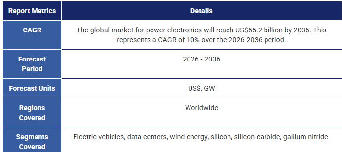
パワーエレクトロニクスの需要は、主に電気自動車(EV)およびデータセンターの需要に牽引され、今後10年間で急速に拡大すると予想されます。IDTechExは、パワーエレクトロニクス市場が2036年までに652億米ドル規模に成長し、予測期間中の年平均成長率(CAGR)は10%になると予測しています。
パワーエレクトロニクス市場全体において、OEM各社は、パワーエレクトロニクス部品に対し、効率の向上、一貫した信頼性、および高出力密度を求めています。 これは、シリコンカーバイド(SiC)や窒化ガリウム(GaN)といったワイドバンドギャップ(WBG)半導体への移行を意味しています。これらの技術は、高電圧動作や、電気自動車の800V e-パワートレインや800VDCデータセンターといった新たな電力アーキテクチャを可能にし、パワーエレクトロニクス業界に革命をもたらす可能性を秘めています。
IDTechExのレポート『パワーエレクトロニクス市場 2026-2036:データセンター、電気自動車、再生可能エネルギー』では、シリコン、炭化ケイ素、窒化ガリウム、および超広バンドギャップ(UWBG)半導体であるダイヤモンド、酸化ガリウム(Ga₂O₃)、窒化アルミニウムをベンチマークし、比較しています。 本レポートでは、EV、データセンター、再生可能エネルギー産業における各半導体材料の利点に加え、導入の障壁や技術革新についても考察しています。また、用途(電気自動車、データセンター、風力発電)および半導体技術(Si、SiC、GaN)ごとに分類した、電力(GW)および市場規模(米ドル)に関する詳細な予測も掲載されています。
.png)
2036年までにSiCがパワーエレクトロニクス産業の過半数のシェアを占める見込みであり、今後10年間でGaNパワーエレクトロニクスの採用が大幅に拡大する。
半導体材料および製造動向
ワイドバンドギャップ半導体技術は、過去10年間で急速に商用化が進みました。SiCとGaNは、ニッチな用途から主流へと移行しています。これらのワイドバンドギャップ半導体材料は、パワーエレクトロニクスの次世代イノベーションにおいて不可欠であり、回路の小型化と高出力化を可能にします。
パワーエレクトロニクスのサプライチェーンは複雑であり、多岐にわたるティア1メーカーと単一材料のウェハーファブが混在している。 シリコンカーバイド(SiC)市場は近年、中国のSiCメーカー間の激しい競争を契機として変革期を迎えています。その結果、SiCウェハーの価格は劇的に低下し、SiCの供給過剰という課題が生じました。本レポートでは、中国を代表するSiCメーカーからの詳細な知見を盛り込み、それらをSiCサプライチェーン全体に位置づけています。
窒化ガリウム(GaN)についても、今後10年間で大幅な発展が見込まれており、300mm GaN-on-Siの商用化や、高電圧GaN用途向けの垂直GaN(vGaN)技術の開発といった重要な進展が予想されます。 予測期間中、IDTechExは世界のGaN生産量が拡大し、GaNコストが低下すると見込んでおり、GaNウェハーの価格はシリコンの価格に近づくと予測しています。GaNとSiCの適用分野がますます重なり合う中、IDTechExは予測期間中にGaNパワーエレクトロニクス市場が大幅に成長すると予想しています。
.png)
Si、WBG、UWBG向け半導体材料における技術革新、ならびに電気自動車、データセンター、再生可能エネルギー分野におけるイノベーションに関する短期、中期、長期のロードマップ。
独自の経験と視点
IDTechExは、新興技術市場を網羅し、半導体材料および電気自動車を専門とする点で、このテーマを扱う上で他に類を見ない強みを持っています。IDTechExの幅広いEV関連ポートフォリオには、バッテリー、熱管理、電気モーター、パワーエレクトロニクスが含まれており、10年以上にわたる業界調査の経験に基づいています。 さらに、IDTechExの最新調査では、急速に進化するデータセンター業界を注視するとともに、再生可能エネルギー分野についても継続的にカバーしています。IDTechExは、パワーエレクトロニクス業界を網羅する深さと広さを兼ね備えた知見を有しており、パワーエレクトロニクス市場および主要な半導体材料に関する重要な洞察を抽出しています。
主なポイント
本レポートは、パワー半導体材料および主要なパワーエレクトロニクス用途に関する重要な市場情報を提供します。これには以下が含まれます
パワーエレクトロニクス材料および製造に関するレビュー
電気自動車、データセンター、再生可能エネルギー向けパワーエレクトロニクスの最新動向
包括的な市場分析
目次
1. 概要
1.1. 技術入門:パワーエレクトロニクスとは?
1.2. パワーエレクトロニクスにおけるトランジスタの重要な特性
1.3. 半導体材料特性の比較
1.4. Siと広帯域ギャップ半導体(SiCおよびGaN)の比較
1.5. EV、データセンター、再生可能エネルギー向けパワーエレクトロニクスの主要な動向
1.6. SiCおよびGaNの製造技術は成熟、UWBGの製造は依然として活発な研究開発段階
1.7. パワーエレクトロニクスのバリューチェーン
1.8. EV用PoEコンポーネントの要件の違いが材料選定に影響
1.9. IDTechExによるインバータの電力密度に関する見通し
1.10. 800V EVプラットフォームは充電速度を向上させ、SiCによって支えられている
1.11. AIはデータセンターを、単なる効率化だけでなく、より高い電力密度へと向かわせている
1.12. 400VAC→800VDCデータセンター:電力密度に牽引され、EVの影響を受ける
1.13. 800VDCデータセンターアーキテクチャにおける主な変化
1.14. NVIDIAは、新しいデータセンター向けに多数のWBG Tier 1企業と提携
1.15. 「スパイク状」のAIトレーニング負荷への対応には、業界を超えた連携が必要
1.16. 太陽光および風力エネルギーは、中国が主導する重要な成長分野
1.17. より強力な風力タービンには、電力アーキテクチャの変更が必要
1.18. 太陽光および風力分野における重要な合併、買収、および合弁事業
1.19. PoE 市場は全体で年平均成長率 10%となり、GaN および SiC の成長が最も著しい。
1.20. EV は引き続きパワーエレクトロニクス市場のシェアの大半を占める。
1.21. 2026年から2036年にかけて、SiCの力強い成長と GaN の急速な商用化が見込まれる。
1.22. アナリストの見解
1.23. IDTechExのサブスクリプションでさらに詳しい情報をご覧いただけます
2. パワーエレクトロニクスの概要
2.1. 技術入門:パワーエレクトロニクスとは?
2.2. パワーエレクトロニクス開発の包括的な目標
2.3. ベアダイ、ディスクリート、およびモジュール
2.4. パワーエレクトロニクスにおけるシリコン
2.5. パワーエレクトロニクスにおける炭化ケイ素(SiC)および窒化ガリウム(GaN)
2.6. 電気自動車への応用:インバータ
2.7. 電気自動車への応用:車載充電器
2.8. 電気自動車への応用:DC-DC コンバータ
2.9. データセンターへの応用
2.10. 風力発電への応用
2.11. パワーエレクトロニクスは系統レベルの安定性にとって極めて重要である
3. パワーエレクトロニクス用半導体
3.1. シリコン(Si)
3.1.1. シリコンは50年以上にわたり主要な半導体として選ばれてきた
3.1.2. シリコンデバイスは数十年にわたり改良されてきた
3.1.3. シリコンの価格は過去50年間で劇的に低下し、現在では圧倒的に安価な選択肢となっている
3.1.4. 次世代パワーエレクトロニクス用途において、シリコンには根本的な限界がある
3.1.5. 電圧やスイッチング周波数が制約となる場合、WBGがSiを補完する
3.2. WBG半導体:炭化ケイ素(SiC)および窒化ガリウム(GaN)
3.2.1. SiC は、シリコンよりもはるかに高い電圧に対応できる
3.2.2. SiC デバイスは、より薄いドリフト層でより高い電圧を処理できる
3.2.3. 多くのパワーエレクトロニクス用途で SiC への移行が見られる
3.2.4. GaN は SiC よりもさらに高いバンドギャップを持ち、電子移動度が非常に高い
3.2.5. バルク GaN は高電圧に対応可能ですが、そのコストは法外なほど高額です
3.2.6. SiC と GaN は、Si IGBT と比較してスイッチング損失を低減します
3.2.7. SiC および GaN には、大幅な改善の余地があります
3.2.8. SiC と GaN は、さまざまな用途において Si を補完する可能性が高いです
3.2.9. さまざまな性能指標(FoM)のスコアは、Si に対して WBG 材料が優位であることを示している
3.2.10. Si IGBT と SiC MOSFET の価格比較
3.2.11. SiC と GaN デバイスのコスト比較
3.2.12. SiC が GaN に「勝った」理由、および今後 10年間でこれが変わる可能性がある理由
3.2.13. SWOT分析:WBG半導体としてのSiC
3.2.14. SWOT分析:WBG半導体としてのGaN
3.3. 超広バンドギャップ半導体:Ga2O3、ダイヤモンド、およびAlN
3.3.1. 超広バンドギャップ(UWBG)半導体とは?
3.3.2. UWBG半導体は多くのPoEアプリケーションに革新をもたらす可能性がある
3.3.3. 3つの主要なUWBG材料間で競争が存在する
3.3.4. AlNおよびAl(Ga)N
3.3.5. 酸化ガリウム(Ga2O3)
3.3.6. ダイヤモンド
3.3.7. UWBG半導体と既存材料の比較
3.3.8. 一部の大手企業がウェハー成長に関与しているが、アプリケーション分野は主にスタートアップやスピンアウト企業が支配している
3.3.9. 防衛部門は UWBG 材料およびアプリケーションの研究に投資している
3.3.10. UWBG には大きな破壊的潜在力があるが、まだ商用化されていない
3.3.11. UWBG ウェハーのコストは低下しつつあるが、依然として法外なほど高価である
3.3.12. UWBGは、商用化前に重要な課題を克服しなければならない
3.3.13. 学界におけるUWBG研究への強力な推進
3.3.14. REWIRE:英国を拠点とするイノベーション・ナレッジ・センター(IKC)
3.3.15. ATECOM Technology が UWBG の主要材料とデバイスを展示
3.3.16. JBDianet は、航空宇宙および防衛用途における CVD ダイヤモンドに期待を寄せる
3.3.17. 旭ダイヤモンドは UWBG およびダイヤモンド半導体に注目
3.3.18. SWOT 分析:UWBG 半導体としてのダイヤモンド
3.3.19. SWOT分析:UWBG半導体としてのGa2O3
4. 半導体製造
4.1. 半導体のバリューチェーン
4.1.1. 概要:原材料から最終ダイまで
4.1.2. 主要企業を含むSiCのバリューチェーン
4.1.3. 主要企業を含むGaNのバリューチェーン
4.1.4. パワーエレクトロニクスサプライヤーの市場シェア
4.1.5. 自動車用GaNデバイスのサプライヤーが増加している
4.2. バルク基板、エピタキシー、および成長法
4.2.1. Si IGBTの製造:原材料から最終製品まで
4.2.2. SiC MOSFETの製造:原材料から最終製品まで
4.2.3. SiC専用装置(1)
4.2.4. SiC 専用装置 (2)
4.2.5. プロセスのエネルギー需要:Si対GaN
4.2.6. 「完璧な」エピタキシーには、多くの科学的および経済的な考慮事項が関わっている
4.2.7. ヘテロエピタキシーとホモエピタキシーには、それぞれ長所と短所がある
4.2.8. GaN にはどの基板が主流となるか?
4.2.9. エピタキシー法:MOCVD-速度と精度のバランス
4.2.10. エピタキシー法:HVPE-テンプレートおよび基板の高速成長
4.2.11. エピタキシー法:MBE-時間はかかるが、非常に正確
4.2.12. エピタキシー法:MPCVD-電気グレードダイヤモンドの標準
4.2.13. エピタキシー法:Mist-CVD-Ga2O3 膜への潜在的な低コストルート
4.2.14. Element 3-5 GmbH の次世代エピタキシー (NLE) は、10 倍のスループットを約束する
4.2.15. Element 3-5 の NLE が成功すれば、エピタキシー業界に大きな変革をもたらす可能性がある
4.2.16. NLE が普及するには、いくつかの課題に対処しなければならない
4.2.17. 純度と成長速度のトレードオフが、商用化の妨げとなっている
4.3. SiC および GaN 製造の最近の動向
4.3.1. SiC における 150mm から 200mm への移行は、コスト面でのメリットと関連している
4.3.2. 200mm ウェーハのダイ数における優位性
4.3.3. 2025年:8インチSiCウェハへの移行は加速し続けている
4.3.4. 世界における200mm SiCウェハの生産
4.3.5. 中国の強力な競争によりSiC価格は下落したが、欧米は追いつくのに苦労した
4.3.6. 多くのパワー半導体サプライヤーは垂直統合されているが、供給を補うために依然として中国に依存している
4.3.7. Synlightは多くの大手ティア1企業に供給しており、300mm SiCへの準備を進めている
4.3.8. TYSiCは中国最大、世界第3位のSiCエピタキシーサプライヤーである
4.3.9. CrystalYondは300mm SiCの研究開発に携わっている
4.3.10. Atecom は、その高度に多様化した材料供給品目に SiC を加えている
4.3.11.Jhonghuan は、シリコンだけに留まらないポートフォリオの多様化を図るため、SiC(および GaN)を追加した
4.3.12.300mm SiC は登場したが、コストが高すぎ、加工技術もまだ整っていない
4.3.13. Bosch は、200mm SiC ウェハーのみを使用する SiC ロードマップに注力している
4.3.14.Bosch は、高度なアーキテクチャへの移行を容易にするトレンチ設計に賭けている
4.3.15.デンソー:SiC 結晶の成長速度向上のための研究開発
4.3.16.Siltectra:コールドスプリット技術
4.3.17.SOITEC の SmartSiC テクノロジー
4.3.18. SmartSiCの利点の概要
4.3.19. 住友金属鉱山:SiCkrest
4.3.20. 住友金属鉱山:SiCkrest (2)
4.3.21. トレンチ対プレーナ
4.3.22. 300mm GaN-on-Siの商用化に向けた広範な連携
4.3.23. インフィニオンは、300mm GaN 分野でのリーダーシップ確立に向けて独自に開発を進めている
4.3.24. パワー・インテグレーションズは、1250V および 1700V の PowiGaN カスケードデバイスを開発
4.3.25. エンジニアリング基板上の垂直 GaN FinFET を先駆けるスタートアップ企業
4.3.26. オンセミは、垂直 GaN デバイスに関する研究を発表
4.3.27. GaN パワー用 Qromis エンジニアリング基板:QST
4.3.28. 垂直型 GaN デバイスがパワーエレクトロニクス市場に革新をもたらす理由
5. EV におけるパワーエレクトロニクス
5.1. 電気自動車の概要
5.1.1. 電気自動車の定義
5.1.2. 電気自動車:代表的な仕様
5.1.3. 排出ガス削減を目指す EU の目標
5.1.4. パワートレインの排気ガス比較
5.2. 電気自動車におけるパワーエレクトロニクスの概要
5.2.1. 電気自動車におけるパワーエレクトロニクスの利用
5.2.2. インバータ、OBC、DC-DC コンバータ
5.2.3. SiC パワーデバイスの限界
5.2.4. OBC技術としてGaNが主流に
5.3. 車載充電器
5.3.1. OBCの現状
5.3.2. OBCへのGaNの導入方法
5.3.3. GaN Systemsの車載充電器
5.3.4. GaN OBCのコスト削減と小型化
5.3.5. リカルド:自動車市場におけるGaN
5.3.6. GaNの様々な用途における進展
5.4. トラクションインバータ
5.4.1. インバータの概要
5.4.2. 従来のEV用インバータ
5.4.3. ディスクリート部品とモジュール
5.4.4. インバータ部品とコスト
5.4.5. 現在のインバータ市場動向
5.4.6. インバータにおけるGaNとSiCの可能性の比較
5.4.7. 電気自動車用インバータのベンチマーク
5.4.8. インバータパッケージに対するSiCの影響
5.4.9. 電力密度に関するIDTechExのインバータ予測
5.5. EVパワーエレクトロニクスに影響を与えるトレンド
5.5.1. パワーエレクトロニクスの効率向上
5.5.2. 効率と熱的利点、800V
5.5.3. 自動車産業におけるSiCの活用例
5.5.4. SiCによる800Vプラットフォームの推進
5.5.5. 800V充電速度
5.5.6. 800VプラットフォームにおけるSiCおよびSi IGBTインバータ
5.5.7. ハイブリッドスイッチインバータ
5.5.8. ハイブリッドスイッチインバータ
5.5.9. パワーエレクトロニクスの統合
5.5.10. トラクション統合型車載充電器(iOBC)
5.5.11. ボルグワーナー:インバータとDC-DCコンバータの統合
5.5.12. SiC MOSFET対Si IGBT:車両総コスト
5.5.13. 自動車OEMおよびサプライヤーによるSiC MOSFETの使用状況-主要OEM
5.5.14. 主要OEM向けSi IGBTサプライヤー
5.5.15. 半導体材料別EVパワーエレクトロニクス予測
5.5.16. 半導体および用途別EVパワーエレクトロニクス市場予測
6. データセンターにおけるパワーエレクトロニクス
6.1. データセンターの概要
6.1.1. データセンターとは?
6.1.2. データセンターの各種タイプ
6.1.3. オンプレミス型データセンターの人気は低下し、ハイパースケーラーとエッジが主流に
6.1.4. データセンターは世界のエネルギーの相当な割合を消費しており、その割合は増加傾向にある
6.1.5. データセンター分野では米国が圧倒的な首位を占め、ドイツ、英国がそれに続く
6.1.6. データセンターの効率は2007年以降向上してきたが、2018年以降は停滞している
6.1.7. 将来のデータセンターの改善には、効率だけでなく電力密度も関わる
6.1.8. コロケーションおよびハイパースケーラープロバイダー、ならびにデータセンタープロバイダーの概要
6.2. データセンターにおけるパワーエレクトロニクスの概要
6.2.1. データセンターアーキテクチャに関する補足
6.2.2. パワーエレクトロニクスはデータセンターの運用において極めて重要な役割を果たす。
6.2.3. 既存のラックアーキテクチャ 1:「シェルフあたり1台のPSU」
6.2.4. 既存のラックアーキテクチャ2:「中央PSUシェルフと48Vバス」
6.3. 力率改善(PFC)と電源ユニット(PSU)
6.3.1. 電源ユニットは、データセンターの効率と電力密度にとって極めて重要である
6.3.2. 力率改善は、パワーエレクトロニクスの重要な用途である
6.3.3. 「80 Plus」プログラムは、PSUの効率に関する世界標準を定めている
6.3.4. その他のプログラムも、世界的に効率要件を奨励または義務付けている
6.3.5. LLCコンバータは電圧をサーバーレベルまで降圧する
6.3.6. PSUにおけるSiCおよびGaNの採用
6.3.7. PSUにおけるWBG採用のタイムライン
6.4. AIデータセンターと800VDC
6.4.1. AIの計算コストは莫大である
6.4.2. 電力と冷却は現在、AIデータセンターの検討事項の最前線にある
6.4.3. AIは、単なる効率化だけでなく、電力密度の向上を推進している
6.4.4. NVIDIAのGB200 NVL72およびGB300 NVL72
6.4.5. 既存のデータセンターアーキテクチャでは将来のサーバー世代に対応できない(1)
6.4.6. 既存のデータセンターアーキテクチャでは将来のサーバー世代に対応できない(2)
6.4.7. NVIDIAによる電力の再配分
6.4.8. 800VDCデータセンターアーキテクチャにおける主な変更点
6.4.9. ラックレベルの 800VDC と資材の削減
6.4.10. EV 充電アーキテクチャが 800VDC データセンターの電力アーキテクチャに与える影響 (1)
6.4.11. EV 充電アーキテクチャが 800VDC データセンターの電力アーキテクチャに与える影響 (2)
6.4.12. NVIDIA の Kyber アーキテクチャは 2027 年に展開が開始される
6.4.13. SST による長期的なデータセンター電力アーキテクチャの簡素化
6.4.14. 2 種類の 800V ラックアーキテクチャにより、既存のデータセンター内の柔軟性が向上
6.4.15. 800VDC は段階的に導入および後付けが可能
6.4.16. NVIDIA は、新しいデータセンター向けに多数の WBG Tier 1 企業と提携
6.4.17. Navitas:GeneSiC と GaNSafe を組み合わせた PSU
6.4.18. Infineon:過渡負荷用のエネルギーバッファを備えた 12kW 高電力密度 PSU
6.4.19. Onsemi:AI およびクラウド向けの 12kW PSU、SiC カスケード JFET を採用
6.4.20. STM:2600W/in3 の効率を実現する 800VDC データセンター向け LLC コンバータ
6.4.21. Innoscience、電力変換にオール GaN 技術を採用
6.4.22. Power Integrations の 1250V/1700V GaN 技術が効率を最大化
6.4.23. 次世代 8~12kW 電源ユニットの概要
6.4.24. AIには本当にこれほどの電力が必要なのか?
6.4.25. なぜより高い電圧を採用しないのか?
6.4.26. 半導体材料別データセンター用パワーエレクトロニクスの予測
6.4.27. データセンター 800VDC (HVDC) 市場の予測
6.5. 「スパイク状」のAIトレーニング負荷
6.5.1. 同期化されたGPUがワークロード管理に新たな課題をもたらす
6.5.2. 変動するAIワークロードはコンピューティング機器に負荷をかけ、電力網に影響を与える
6.5.3. ソフトウェアのみによる緩和策
6.5.4. GPU電力平滑化
6.5.5. GPU電力平滑化の課題と限界
6.5.6. ラックレベルのエネルギー貯蔵
6.5.7. 3つのソリューションすべての概要
6.5.8. 電力の安定化には、3つのソリューションすべてと業界全体の協力が必要
7. 再生可能エネルギーにおけるパワーエレクトロニクス
7.1. 再生可能エネルギーの紹介
7.1.1. 再生可能エネルギーとは?
7.1.2. 過去10年間で風力および太陽光発電は大幅に成長した
7.1.3. 風力および太陽光発電の価格は近年大幅に低下している
7.1.4. 風力発電の地域別内訳(2015-2024年)
7.1.5. 太陽光発電の地域別内訳(2015-2024年)
7.1.6. 導入規模とコストの両面で陸上風力が主流
7.1.7. 太陽光発電の各種タイプ
7.1.8. 太陽光発電用パワーエレクトロニクスのバリューチェーン
7.1.9. 風力発電用パワーエレクトロニクスのバリューチェーン
7.1.10. 太陽光・風力分野における主要な合併、買収、および合弁事業
7.2. 風力発電におけるパワーエレクトロニクス
7.2.1. 2026年から2036年までの風力タービン容量の成長予測
7.2.2. 風力タービンのナセル
7.2.3. 風速は一定ではありませんが、AC出力は一定でなければなりません
7.2.4. 固定速度風力タービン(主に旧式)
7.2.5. 二重給電誘導発電機(DFIG)
7.2.6. 永久磁石同期発電機およびフルパワーコンバータ
7.2.7. DFIGとフルコンバージョン方式の比較
7.2.8. 現代の風力タービンにおけるDFIGとPMSGの比較
7.2.9. 高出力域ではPMSGとフルコンバージョンが主流
7.2.10. 2026年から2036年にかけてPMSGの優位性がさらに高まると予想
7.2.11. 2026年から2036年にかけて導入されるPMSG搭載の新規風力タービンとDFIG搭載の新規風力タービンの予測
7.2.12. PMSG タービン用フルパワーコンバータ
7.2.13. シリコン IGCT 技術に基づく日立の最高出力コンバータ
7.2.14. IGBT 技術に基づく ABB の低出力コンバータ
7.2.15. Ingeteam のフルコンバータは最大 18MW をサポート
7.2.16. コンバータ向けに最適化されたInfineonの2つのデュアル IGBT パワーモジュール
7.2.17. 既存の風力発電用コンバータおよびパワーモジュールの概要
7.2.18. 風力発電用コンバータに関する Hopewind と Wolfspeed の提携
7.2.19. コンバータタイプ別の風力発電用電子機器の予測
7.2.20. 半導体材料別の風力発電コンバータ予測
7.3. 洋上風力発電における電圧源型コンバータ(VSC-HVDC)
7.3.1. VSC-HVDCとは?
7.3.2. 洋上風力発電におけるACに対するHVDCの利点
7.3.3. 世界のHVDC風力発電所プロジェクトのマップ
7.3.4. VSC-HVDCは確立されたシリコンIGBT技術に依存している
8. 予測
8.1. 調査方法
8.2. 半導体材料別パワーエレクトロニクス市場予測(2023-2036年)
8.3. 用途分野別パワーエレクトロニクス市場全体予測
8.4. 半導体材料別電気自動車(EV)用パワーエレクトロニクス予測
8.5. 半導体および用途別EV用パワーエレクトロニクス市場予測
8.6. 半導体材料別データセンター用パワーエレクトロニクス予測
8.7. データセンター 800VDC (HVDC) 市場予測
8.8. コンバータタイプ別風力発電用パワーエレクトロニクス予測
8.9. 半導体材料別風力発電用コンバータ予測
9. 企業プロファイル
9.1. AcBel Polytech Inc.
9.2. 旭ダイヤモンド工業株式会社
9.3. Atecom Technology Co.,Ltd.
9.4. BMW
9.5. Bosch Semiconductors
9.6. BYD Auto
9.7. Diamond Foundry:電気自動車用インバータ
9.8. Efficient Power Conversion:GaN FET
9.9. Efficient Power Conversion:自動車向けGaN
9.10. Element 3-5 GmbH
9.11. Gallox Semiconductors
9.12. Hebei Synlight Semiconductor
9.13. Hitachi Energy Ltd.
9.14. Hyundai
9.15. Infineon:車載充電器向け750V SiC MOSFET
9.16. インフィニオン:自動車用パワーエレクトロニクス
9.17. インフィニオン:SiC OEM パートナーシップの拡大
9.18. JB Dianet LLP
9.19. Leguan
9.20. Nexperia:EV パワーエレクトロニクス向け GaN
9.21. Novomorphic
9.22. QPT:MHz スイッチング、アクティブ冷却 GaN
9.23. Silanna UV
9.24. Silicon Austria Labs GmbH
9.25. Transphorm(ルネサス):高電力用途向け GaN
9.26. TYSiC
9.27. Wolfspeed:主要な SiC 供給契約
9.28. Zhonghuan Advanced Semiconductor Technology Co., Ltd.

Summary
Ten-year power electronics market forecasts, including forecasts for electric vehicles, data centers, and renewable energy. Detailed comparison of silicon, silicon carbide, gallium nitride, and ultra-wide bandgap semiconductors.
The demand for power electronics is expected to grow rapidly over the next ten years, driven largely by demand in electric vehicles (EVs) and data centers. IDTechEx expects the power electronics market to grow to US$65.2 billion by 2036, representing a 10% CAGR over the forecasting period.
Across the power electronics market, OEMs are pushing for increased efficiency, consistent reliability, and greater power density from their power electronics components. Increasingly, this means turning to wide bandgap (WBG) semiconductors: silicon carbide (SiC) and gallium nitride (GaN). These technologies have the potential to revolutionize the power electronics industry, enabling high-voltage operation and new power architectures, such as the 800V e-powertrain in electric vehicles and 800VDC data centers.
IDTechEx's report "Power Electronics Market 2026-2036: Data Centers, Electric Vehicles, and Renewables" benchmarks and compares silicon, silicon carbide, gallium nitride and ultra-wide bandgap (UWBG) semiconductors diamond, gallium oxide (Ga2O3) and aluminum nitride. The report considers the merits of each semiconductor material across the EV, data center, and renewables industries, as well as barriers to adoption and technological innovations. The report includes granular forecasts detailing power (GW) and market size (US$) segmented by application (electric vehicles, data centers, and wind energy), and by semiconductor technology (Si, SiC, GaN).
SiC will take the majority share of the power electronics industry by 2036, with significant uptake of GaN power electronics over the next ten years.
Semiconductor materials and manufacture trends
Wide bandgap semiconductor technology has commercialized rapidly over the past ten years. SiC and GaN have moved from niche applications into the mainstream. These wide bandgap semiconductor materials are critical for the next generation of innovations in power electronics, enabling smaller circuits and higher power.
The power electronics supply chain is complex, with a combination of highly-diversified tier 1 manufacturers and single-material wafer fabs. The silicon carbide market has undergone a period of transformation in recent years, catalyzed by aggressive competition between Chinese SiC manufacturers. The price of SiC wafers has decreased dramatically as a result, and SiC oversupply challenges arose. This report includes detailed insights from leading Chinese SiC manufacturers and maps them onto the overall SiC supply chain.
Gallium nitride is also expected to develop significantly over the next ten years, with key events such as the commercialization of 300mm GaN-on-Si, and the development of vertical GaN (vGaN) technology for high-voltage GaN applications. Over the forecasting period, IDTechEx expects global GaN production volume to increase and GaN costs to decrease, with GaN wafer prices forecast to approach those of silicon. With the application areas available to GaN and SiC increasingly overlapping, IDTechEx anticipates that the GaN power electronics market will grow significantly in the forecasting period.
Short-, medium-, and long-term roadmap of technology innovations in semiconductor materials for Si, WBG and UWBG, as well as innovations in electric vehicles, data centers, and renewable energy.
Unique experience and perspective
IDTechEx is uniquely well-positioned to cover this topic, covering emerging technology markets, specializing in semiconductor materials and electric vehicles. IDTechEx's broad EV portfolio includes batteries, thermal management, e-motors and power electronics, and builds upon over a decade of experience covering the industry. Moreover, IDTechEx's latest research monitors the rapidly evolving data center industry alongside continual coverage of the renewable energy sector. IDTechEx has the depth and breadth of knowledge to capture the power electronics industry, and distil key insights on the power electronics market and key semiconductor materials.
Key Aspects
This report provides critical market intelligence on power semiconductor materials and key power electronics applications. This includes
A review of power electronics materials and manufacture
Latest developments in power electronics for electric vehicles, data centers, and renewables
Comprehensive market analysis
Table of Contents
1. EXECUTIVE SUMMARY
1.1. Technical primer: What is power electronics?
1.2. Important properties of a transistor in power electronics
1.3. Comparison of semiconductor material properties
1.4. Comparison of Si to wide bandgap semiconductors SiC and GaN
1.5. Key trends in power electronics for EVs, data centers, and renewables
1.6. Manufacturing for SiC and GaN refined; UWBG manufacture still active R&D
1.7. The power electronics value chain
1.8. Different EV PoE component requirements affect the materials used
1.9. IDTechEx inverter outlook on power density
1.10. 800V EV platforms improves charging speeds and is supported by SiC
1.11. AI pushes data centers towards higher power density, not just efficiency
1.12. 400VAC → 800VDC data centers: driven by power density, influenced by EVs
1.13. Key changes in the 800VDC data center architecture
1.14. NVIDIA partners with numerous WBG Tier 1s for new data centers
1.15. Dealing with "spiky" AI training loads requires cross-industry collaboration
1.16. Solar and wind energy are significant growth areas led by China
1.17. More powerful wind turbines necessitate a change in power architecture
1.18. Significant mergers, acquisitions, and joint ventures in solar and wind
1.19. Overall 10% CAGR in PoE market, with strongest growth in GaN and SiC.
1.20. EV continues to take majority of power electronics market share
1.21. Strong SiC growth and rapid GaN commercialization expected 2026-2036
1.22. Analyst opinions
1.23. Access more with an IDTechEx subscription
2. INTRODUCTION TO POWER ELECTRONICS
2.1. Technical primer: What is power electronics?
2.2. Overarching goals of power electronics development
2.3. Bare dies, discretes, and modules
2.4. Silicon in power electronics
2.5. Silicon carbide (SiC) and gallium nitride (GaN) in power electronics
2.6. Electric vehicle applications: Inverter
2.7. Electric vehicle applications: On-board charger
2.8. Electric vehicle applications: DC-DC converter
2.9. Data center applications
2.10. Applications in wind energy
2.11. Power electronics are critical for grid-level stability
3. SEMICONDUCTORS FOR POWER ELECTRONICS
3.1. Silicon (Si)
3.1.1. Silicon has been the semiconductor of choice for over fifty years
3.1.2. Silicon devices have been refined over decades
3.1.3. Silicon has decreased in price dramatically over fifty years and is by far the cheapest option
3.1.4. Silicon is fundamentally limited in next generation power electronics applications
3.1.5. WBGs will complement Si where voltages/switching frequencies are limiting
3.2. WBG semiconductors: Silicon carbide (SiC) and gallium nitride (GaN)
3.2.1. SiC can support considerably higher voltages than silicon
3.2.2. SiC devices can handle higher voltages with a thinner drift layer
3.2.3. The switch to SiC is seen in many power electronics applications
3.2.4. GaN has an even higher bandgap than SiC, and a very high electron mobility
3.2.5. Bulk GaN can reach high voltages, but is prohibitively expensive
3.2.6. Both SiC and GaN reduce switching losses compared to Si IGBTs
3.2.7. SiC & GaN have substantial room for improvement
3.2.8. SiC and GaN are likely to complement Si in various different applications
3.2.9. Different figure of merit (FoM) scores show WBG material dominance over Si
3.2.10. Si IGBT and SiC MOSFET Price Comparison
3.2.11. SiC and GaN Device Cost Comparison
3.2.12. Why SiC "won" over GaN, and why this could change in the next ten years
3.2.13. SWOT analysis: SiC as a WBG semiconductor
3.2.14. SWOT analysis: GaN as a WBG semiconductor
3.3. Ultra-wide bandgap semiconductors: Ga2O3, diamond, and AlN
3.3.1. What are ultra-wide bandgap (UWBG) semiconductors?
3.3.2. UWBG semiconductors could disrupt many PoE applications
3.3.3. There is competition between three different key UWBG materials
3.3.4. AlN and Al(Ga)N
3.3.5. Gallium oxide (Ga2O3)
3.3.6. Diamond
3.3.7. Comparison of UWBG semiconductors to existing materials
3.3.8. Some larger players are involved in wafer growth, but applications are largely dominated by startups and spinouts
3.3.9. The defense sector is investing in UWBG material and applications research
3.3.10. UWBGs have huge disruptive potential, but are not yet commercial
3.3.11. UWBG wafer costs are coming down, but are still prohibitively expensive
3.3.12. UWBGs must overcome key challenges before commercialization
3.3.13. Strong push towards UWBG research in academia
3.3.14. REWIRE: A UK-based innovation and knowledge center (IKC)
3.3.15. ATECOM Technology showcase key UWBG materials and devices
3.3.16. JBDianet is hopeful for CVD diamond in aerospace and defense applications
3.3.17. Asahi Diamond looks towards UWBG and diamond semiconductors
3.3.18. SWOT analysis: Diamond as an UWBG semiconductor
3.3.19. SWOT analysis: Ga2O3 as an UWBG semiconductor
4. SEMICONDUCTOR MANUFACTURE
4.1. The semiconductor value chain
4.1.1. Overview: From raw materials to final die
4.1.2. SiC Value Chain with Key Players
4.1.3. GaN Value Chain with Key Players
4.1.4. Market share of power electronics suppliers
4.1.5. Automotive GaN device suppliers are growing
4.2. Bulk substrates, epitaxy, and growth methods
4.2.1. Si IGBT production: Raw materials to end-product
4.2.2. SiC MOSFET Production: Raw materials to end-product
4.2.3. SiC-specific equipment (1)
4.2.4. SiC-specific equipment (2)
4.2.5. Energy demand of processes: Si vs GaN
4.2.6. Many scientific and economic considerations feed into the "perfect" epitaxy
4.2.7. Heteroepitaxy and homoepitaxy both come with advantages and drawbacks
4.2.8. Which substrate will prevail for GaN?
4.2.9. Epitaxy methods: MOCVD - a balance of speed and precision
4.2.10. Epitaxy methods: HVPE - for fast template and substrate growth
4.2.11. Epitaxy methods: MBE - slow, but highly accurate
4.2.12. Epitaxy methods: MPCVD - the standard for electrical-grade diamond
4.2.13. Epitaxy methods: Mist-CVD - a potential low-cost route to Ga2O3 films
4.2.14. Element 3-5 GmbH's next-level epitaxy (NLE) promises 10x higher throughput
4.2.15. Element 3-5's NLE could prove highly disruptive to epitaxy if successful
4.2.16. Several challenges must be addressed before NLE can take off
4.2.17. Commercialization is limited by a trade-off between purity and growth-rate
4.3. Recent trends in SiC and GaN manufacture
4.3.1. The 150mm to 200mm transition in SiC is associated with cost advantages
4.3.2. 200mm Wafer Die Count Advantage
4.3.3. 2025: The transition to 8-inch SiC wafers continues to accelerate
4.3.4. 200mm SiC wafer production worldwide
4.3.5. Strong Chinese competition drove down SiC prices, while the West struggled to keep up
4.3.6. Many power semiconductor suppliers are vertically integrated, but still rely on China to top up supply
4.3.7. Synlight supplies many leading tier 1s and is readying itself for 300mm SiC
4.3.8. TYSiC is China's largest, and the world's 3rd largest, SiC epitaxy supplier
4.3.9. CrystalYond is involved in the R&D for 300mm SiC
4.3.10. Atecom includes SiC among its highly diversified material supply
4.3.11. Jhonghuan adds SiC (and GaN) to diversify its portfolio beyond just silicon
4.3.12. 300mm SiC is here, but costs are too high and processing is not ready
4.3.13. Bosch commits to SiC roadmap using only 200mm SiC wafers
4.3.14. Bosch bets on trench design for easy transition to advanced architectures
4.3.15. Denso: Research and development for faster SiC crystal growth
4.3.16. Siltectra: Cold split technology
4.3.17. SmartSiC Technology from SOITEC
4.3.18. Summary of SmartSiC Advantages
4.3.19. Sumitomo Metal Mining: SiCkrest
4.3.20. Sumitomo Metal Mining: SiCkrest (2)
4.3.21. Trench vs planar
4.3.22. Extensive collaboration to commercialize 300mm GaN-on-Si
4.3.23. Infineon is working independently to establish leadership in 300mm GaN
4.3.24. Power Integrations develops 1250V and 1700V PowiGaN cascode devices
4.3.25. Startups pioneering vertical GaN FinFETs on engineered substrates
4.3.26. Onsemi announces research on vertical GaN devices
4.3.27. Qromis engineered substrate for GaN power: QST
4.3.28. Why vertical GaN devices could disrupt the power electronics market
5. POWER ELECTRONICS IN EVS
5.1. Introduction to electric vehicles
5.1.1. Electric vehicle definitions
5.1.2. Electric vehicles: Typical specs
5.1.3. EU targets drive down emissions
5.1.4. Powertrain tailpipe emissions comparison
5.2. Overview of power electronics in electric vehicles
5.2.1. Power electronics use in electric vehicles
5.2.2. Inverter, OBC, DC-DC converter
5.2.3. Limitations of SiC power devices
5.2.4. GaN to become preferred OBC technology
5.3. Onboard chargers
5.3.1. Current landscape for OBCs
5.3.2. How GaN is implemented into an OBC
5.3.3. GaN Systems' onboard charger
5.3.4. Cost and volume reductions of a GaN OBC
5.3.5. Ricardo: GaN in the automotive market
5.3.6. Progress of different applications of GaN
5.4. Traction inverters
5.4.1. Inverter overview
5.4.2. Traditional EV inverter
5.4.3. Discretes and modules
5.4.4. Inverter components and cost
5.4.5. Current inverter landscape
5.4.6. GaN vs SiC potential in the inverter
5.4.7. Electric vehicle inverter benchmarking
5.4.8. SiC impact on the inverter package
5.4.9. IDTechEx inverter predictions on power density
5.5. Trends impacting EV power electronics
5.5.1. Improving the efficiency of power electronics
5.5.2. Efficiency and thermal gains, 800V
5.5.3. Examples of SiC in the automotive industry
5.5.4. SiC drives 800V platforms
5.5.5. 800V charging speeds
5.5.6. 800V platforms SiC and Si IGBT inverters
5.5.7. Hybrid switch inverters
5.5.8. Hybrid switch inverters
5.5.9. Integration of power electronics
5.5.10. Traction integrated onboard charger (iOBC)
5.5.11. BorgWarner: Combined inverter and DC-DC converter
5.5.12. SiC MOSFET vs Si IGBT: Overall vehicle cost
5.5.13. SiC MOSFET usage by automotive OEMs and suppliers - leading OEMs
5.5.14. Si IGBT suppliers to leading OEMs
5.5.15. Electric vehicle power electronics forecast by semiconductor material
5.5.16. EV power electronics market forecast by semiconductor and application
6. POWER ELECTRONICS IN DATA CENTERS
6.1. Introduction to data centers
6.1.1. What is a data center?
6.1.2. Different types of data centers
6.1.3. On-site data centers are losing popularity, hyperscalers and edge take over
6.1.4. Data centers consume a significant and growing portion of global energy
6.1.5. The USA leads significantly on data centers, followed by Germany and the UK
6.1.6. Data center efficiency has improved since 2007, but has stalled since 2018
6.1.7. Future data center improvements involve power density, not just efficiency
6.1.8. Summary of colocation and hyperscaler providers, and data center providers
6.2. Overview of power electronics in data centers
6.2.1. Some notes on data center architecture
6.2.2. Power electronics play a critical role in data center operation.
6.2.3. Incumbent rack architecture 1: "One PSU per shelf"
6.2.4. Incumbent rack architecture 2: "Central PSU shelf and 48V bus"
6.3. Power factor correction (PFC) and the power supply unit (PSU)
6.3.1. Power supply units are critical for data center efficiency and power density
6.3.2. Power factor correction is a crucial use of power electronics
6.3.3. The "80 Plus" program sets the global standard for PSU efficiency
6.3.4. Other programs incentivize or mandate efficiency requirements globally
6.3.5. The LLC converter steps voltage down to the server level
6.3.6. Adoption of SiC and GaN in the PSU
6.3.7. Timeline of WBG adoption in PSUs
6.4. AI data centers and 800VDC
6.4.1. Computational costs of AI are huge
6.4.2. Power and cooling are now at the fore of AI data center considerations
6.4.3. AI is driving the push for increased power density, rather than just efficiency
6.4.4. Nvidia's GB200 NVL72 and GB300 NVL72
6.4.5. Existing data center architecture cannot support future server generations (1)
6.4.6. Existing data center architecture cannot support future server generations (2)
6.4.7. NVIDIA's redistribution of power
6.4.8. Key changes in the 800VDC data center architecture
6.4.9. Rack-level 800VDC and material reductions
6.4.10. EV charging architecture influences 800VDC data center power architecture (1)
6.4.11. EV charging architecture influences 800VDC data center power architecture (2)
6.4.12. NVIDIA's Kyber Architecture will begin rollout in 2027
6.4.13. Long-term data center power architecture simplified by SSTs
6.4.14. Two different 800V rack architectures increase flexibility within existing DCs
6.4.15. 800VDC can be implemented gradually and retrofitted
6.4.16. NVIDIA partners with numerous WBG Tier 1s for new data centers
6.4.17. Navitas: Combined GeneSiC and GaNSafe PSU
6.4.18. Infineon: 12kW high power density PSU with energy buffer for transient loads
6.4.19. Onsemi: 12kW PSU for AI and cloud features SiC cascode JFETs
6.4.20. STM: LLC converter for 800VDC data centers with 2600W/in3 efficiency
6.4.21. Innoscience commits to all-GaN technology for power conversion
6.4.22. Power Integrations 1250V/1700V GaN technology maximizes efficiency
6.4.23. Summary of next-generation 8-12kW PSUs
6.4.24. Does AI really need this much power?
6.4.25. Why not go to higher voltages?
6.4.26. Data center power electronics forecast by semiconductor material
6.4.27. Data center 800VDC (HVDC) market forecast
6.5. "Spiky" AI training loads
6.5.1. Synchronized GPUs introduce new challenges in workload management
6.5.2. Fluctuating AI workloads stress compute equipment and affect the grid
6.5.3. Software-only mitigation
6.5.4. GPU power smoothing
6.5.5. Challenges and limitations of GPU power smoothing
6.5.6. Rack-level energy storage
6.5.7. Summary of all three solutions
6.5.8. Power stabilization requires all three solutions and industry-wide cooperation
7. POWER ELECTRONICS IN RENEWABLES
7.1. Introduction to renewables
7.1.1. What is renewable energy?
7.1.2. Wind and solar have grown significantly in the past ten years
7.1.3. Wind and solar prices have dropped significantly in recent years
7.1.4. Geographical breakdown of wind energy generation (2015-2024)
7.1.5. Geographical breakdown of solar energy generation (2015-2024)
7.1.6. Onshore wind dominates, both in rollout and cost
7.1.7. Different types of solar power
7.1.8. Solar energy power electronics value chain
7.1.9. Wind energy power electronics value chain
7.1.10. Significant mergers, acquisitions, and joint ventures in solar and wind
7.2. Power electronics in wind energy
7.2.1. Forecast wind turbine capacity growth from 2026 to 2036
7.2.2. The wind turbine nacelle
7.2.3. Wind speed is not constant, but the AC output must be
7.2.4. Fixed-speed wind turbines (mostly legacy)
7.2.5. Doubly-fed induction generator (DFIG)
7.2.6. Permanent magnet synchronous generators and full power converters
7.2.7. Comparison of DFIG and full conversion
7.2.8. Comparison of DFIG and PMSG in modern turbines
7.2.9. PMSG and full conversion dominates at higher power ratings
7.2.10. PMSG expected to increase dominance from 2026-36
7.2.11. Forecast of new turbines introduced with PMSG vs. DFIG 2026-2036
7.2.12. Full power converter for PMSG turbines
7.2.13. Hitachi's most powerful converter based on silicon IGCT technology
7.2.14. ABB's lower-power converter based on IGBT technology
7.2.15. Ingeteam full converter supports up to 18MW
7.2.16. Infineon's two dual-IGBT power modules optimized for converters
7.2.17. Summary of existing wind power converters and power modules
7.2.18. Hopewind's partnership with Wolfspeed for wind converters
7.2.19. Wind power electronics forecast by converter type
7.2.20. Wind power converter forecast by semiconductor material
7.3. Voltage-source converter HVDC in offshore wind
7.3.1. What is VSC-HVDC?
7.3.2. Benefits of HVDC over AC in offshore wind
7.3.3. Map of global HVDC wind farm projects
7.3.4. VDC-HVDC is reliant on well-established silicon IGBT technology
8. FORECASTS
8.1. Methodology
8.2. Power electronics market forecast by semiconductor material 2023-2036
8.3. Power electronics overall market forecast by application area
8.4. Electric vehicle power electronics forecast by semiconductor material
8.5. EV power electronics market forecast by semiconductor and application
8.6. Data center power electronics forecast by semiconductor material
8.7. Data center 800VDC (HVDC) market forecast
8.8. Wind power electronics forecast by converter type
8.9. Wind power converter forecast by semiconductor material
9. COMPANY PROFILES
9.1. AcBel Polytech Inc.
9.2. Asahi Diamond Industrial Co. Ltd.
9.3. Atecom Technology Co., Ltd.
9.4. BMW
9.5. Bosch Semiconductors
9.6. BYD Auto
9.7. Diamond Foundry: Electric Vehicle Inverters
9.8. Efficient Power Conversion: GaN FETs
9.9. Efficient Power Conversion: GaN in Automotive
9.10. Element 3-5 GmbH
9.11. Gallox Semiconductors
9.12. Hebei Synlight Semiconductor
9.13. Hitachi Energy Ltd.
9.14. Hyundai
9.15. Infineon: 750V SiC MOSFETs for Onboard Chargers
9.16. Infineon: Automotive Power Electronics
9.17. Infineon: Expanding SiC OEM Partnerships
9.18. JB Dianet LLP
9.19. Leguan
9.20. Nexperia: GaN for EV Power Electronics
9.21. Novomorphic
9.22. QPT: MHz Switching, Active Cooling GaN
9.23. Silanna UV
9.24. Silicon Austria Labs GmbH
9.25. Transphorm (Renesas) GaN for high power applications
9.26. TYSiC
9.27. Wolfspeed: Major SiC Supply Deals
9.28. Zhonghuan Advanced Semiconductor Technology Co., Ltd.
ご注文は、お電話またはWEBから承ります。お見積もりの作成もお気軽にご相談ください。本レポートと同分野(通信・IT)の最新刊レポート
IDTechEx社の 自動車 - Electric Vehicles分野 での最新刊レポート
よくあるご質問IDTechEx社はどのような調査会社ですか?IDTechExはセンサ技術や3D印刷、電気自動車などの先端技術・材料市場を対象に広範かつ詳細な調査を行っています。データリソースはIDTechExの調査レポートおよび委託調査(個別調査)を取り扱う日... もっと見る 調査レポートの納品までの日数はどの程度ですか?在庫のあるものは速納となりますが、平均的には 3-4日と見て下さい。
注文の手続きはどのようになっていますか?1)お客様からの御問い合わせをいただきます。
お支払方法の方法はどのようになっていますか?納品と同時にデータリソース社よりお客様へ請求書(必要に応じて納品書も)を発送いたします。
データリソース社はどのような会社ですか?当社は、世界各国の主要調査会社・レポート出版社と提携し、世界各国の市場調査レポートや技術動向レポートなどを日本国内の企業・公官庁及び教育研究機関に提供しております。
|
|