サブ100nm リソグラフィ:市場分析と戦略課題Sub-100nm Lithography: Market Analysis and Strategic Issues 本レポートでは、関連する技術、その発展の可能性、ユーザーが直面している問題や選択、そしてチャンスと落とし穴を調査・予測している。世界市場を分析・予測。i線、DUV、EUV装置メーカーの市場シェアも掲載... もっと見る

サマリー
本レポートでは、関連する技術、その発展の可能性、ユーザーが直面している問題や選択、そしてチャンスと落とし穴を調査・予測している。世界市場を分析・予測。i線、DUV、EUV装置メーカーの市場シェアも掲載しています。
原動力
半導体技術のノードが縮小し、より小型で複雑な半導体デバイスへの需要が高まる中、これらの課題に対応するためのリソグラフィ技術の進歩を後押しする原動力がいくつかある:
技術の微細化:技術的微細化:新しい技術ノードが登場するたびに、半導体メーカーは性能、電力効率、集積度を向上させるため、トランジスタと相互接続のサイズを縮小することを目指しています。このような微細な形状を高精度・高解像度でパターニングするためには、高度なリソグラフィ技術が不可欠であり、次世代リソグラフィツールの開発が推進されています。
EUVリソグラフィの採用:EUVリソグラフィは、従来の光リソグラフィよりも波長が短いため、より微細で複雑なパターンを形成することが可能です。ノードの微細化に伴い、必要なパターニング分解能を達成するためには、EUVリソグラフィの採用がますます必要となっている。
マルチパターニング技術:フィーチャサイズが光リソグラフィの限界に近づくにつれて、セルフアラインド・ダブルパターニング(SADP)、セルフアラインド・クアドラプルパターニング(SAQP)、マルチビーム・マスクレスリソグラフィ(MBML)などのマルチパターニング技術が、所望のフィーチャ密度とピッチを達成するために不可欠となる。これらの技術では、複雑なパターンを形成するために複数の露光工程とエッチング工程が必要となるため、高度なリソグラフィ・ソリューションの必要性が高まっています。
解像度向上技術(RET):パターン転写の解像度と忠実度を向上させるため、リソグラフィ装置には、光学的近接補正(OPC)、位相シフトマスク(PSM)、ソースマスク最適化(SMO)などの解像度向上技術が組み込まれています。
これらのRETは、回折やその他の光学的制限の影響を緩和するのに役立ち、先端ノードでより微細なフィーチャの製造を可能にします。
プロセス制御と歩留まりの改善:フィーチャーサイズが微細化するにつれて、厳密なプロセス制御を維持することがますます難しくなっています。高度なリソグラフィ・ツールには、均一性、オーバーレイ精度、欠陥低減を確実にするための高度な計測およびプロセス制御機能が組み込まれています。これらの機能は、先端ノードで高い歩留まりと製造の一貫性を達成するために不可欠です。
新興アプリケーションと市場需要:人工知能(AI)、5Gコネクティビティ、自律走行車、IoTデバイスなどの新技術は、特定の性能要件を備えた特殊な半導体デバイスの需要を促進している。高度なリソグラフィ・ソリューションは、これらのアプリケーションに必要な複雑な構造や材料をパターニングするために不可欠であり、リソグラフィ技術の革新を促進している。
本レポートの必要性
半導体リソグラフィは、半導体製造の領域における礎石であり、現代の電子機器に電力を供給する複雑な半導体デバイスの作成において極めて重要なプロセスとして機能している。半導体技術の進歩とともにリソグラフィ技術も進化し、解像度、精度、スループットの限界を押し広げ、これまで以上に小さく複雑な半導体構造の製造を可能にしています。この包括的なレポートは、半導体リソグラフィの多面的な状況を掘り下げ、半導体リソグラフィのエコシステムを形成する主要技術、市場動向、業界の課題、将来の展望を探っています。
半導体産業は、より高性能でエネルギー効率の高い電子デバイスの需要に牽引され、微細化のあくなき追求を目の当たりにしている。極端紫外線(EUV)リソグラフィ、マルチパターニング、液浸リソグラフィなどの高度なリソグラフィ技術は、10ナノメートル以下の微細化を実現する上で極めて重要な役割を果たし、半導体製造能力の限界を押し広げています。
半導体リソグラフィ市場は、技術の進歩に加え、市場ダイナミクス、規制政策、業界連携など、無数の要因の影響を受けています。本レポートは、世界の半導体リソグラフィ市場を包括的に分析し、市場規模、成長促進要因、競争環境、新たなビジネスチャンスに関する洞察を提供します。リソグラフィ装置、材料、プロセスの詳細な調査を通じて、関係者は進化する半導体リソグラフィの状況と半導体産業への影響についてより深い理解を得ることができます。
さらに、本レポートでは、マスクの複雑さや欠陥の低減からコスト制約や歩留まりの最適化まで、半導体リソグラフィが直面する主要な課題とボトルネックを探っています。重要な課題と潜在的な解決策を明らかにすることで、関係者はリスクを軽減し、半導体リソグラフィ市場の成長機会を活用するための戦略を考案することができます。
半導体リソグラフィが技術の進歩や市場の要求に応じて進化し続ける中、半導体エコシステム全体の関係者は、業界を形成する最新の動向やトレンドを常に把握しておく必要があります。本レポートは、半導体リソグラフィのダイナミックな状況について実用的な洞察を求める半導体メーカー、装置サプライヤー、投資家、その他の業界関係者にとって貴重なリソースとなります。包括的な分析と戦略的提言を通じて、本レポートは関係者が半導体リソグラフィの複雑な地形をナビゲートし、半導体製造のイノベーションを推進できるよう支援します。
レポート対象範囲
本レポートでは、世界の半導体リソグラフィ市場について、過去のデータ、現在の市場規模、予測される成長動向などを詳細に分析しています。また、技術、エンドユーザー産業、地理的地域に基づく市場細分化も含まれます。
光リソグラフィ、極端紫外線(EUV)リソグラフィ、マルチプル・パターニング、ナノインプリント・リソグラフィなど、半導体製造に利用されるさまざまなリソグラフィ技術を調査します。本セクションでは、各技術の原理、進歩、応用について掘り下げる。
市場セグメンテーション:
本レポートでは、装置タイプ別のリソグラフィベンダーの市場シェア(売上高、出荷台数など)に関する洞察を提供しています。1992年以降のベンダー別市場シェアも掲載しています。
本レポートでは、ノードマイグレーション、中国制裁、新半導体材料(特に炭化ケイ素)など、半導体リソグラフィ市場を牽引する現在および新たなトレンドを特定・分析しています。
目次
目次
第1章 はじめに 1-1
1.1 本レポートの必要性 1-1
第2章 エグゼクティブサマリー 2-1
2.1 主要課題のサマリー 2-1
2.2 市場機会のサマリー 2-2
第3章 リソグラフィの課題と動向 3-1
3.1 光学システム 3-1
3.1.1 はじめに 3-1
3.1.2 ステップ&リピートアライナー 3-8
3.1.3 深紫外線DUV)3-11
3.2 EUV 3-18
3.5 ナノインプリントリソグラフィ 3-23
3.4 X線リソグラフィ 3-28
3.3 電子ビームリソグラフィ 3-34
3.4 イオンビームリソグラフィ 3-38
Chapter4 ユーザーとサプライヤーの戦略 4-1
4.1 リソグラフィニーズの決定 4-1
4.2 ベンダーのベンチマーク 4-3
4.2.1 価格設定 4-3
4.2.2 ベンダーのコミットメントと姿勢 4-5
4.2.3 ベンダーの能力 4-7
4.2.4 システム能力 4-9
4.2.5 装置評価時のベンダーのフィードバック 4-9
4.2.6 装置製造時のベンダーのフィードバック 4-11
4.3 競争環境 4-12
4.4 クラス1クリーンルーム用装置 4-15
4.5 将来工場のための装置 4-18
4.6 機会 4-19
第5章 市場予測 5-1
5.1 ドライビングフォース 5-1
5.1.1 技術動向 5-4
5.1.2 経済動向 5-5
5.1.3 光学的限界 5-9
5.2 市場予測の前提条件 5-10
5.3 市場予測 5-11
図表リスト表
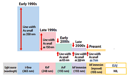
3.1 波長の「世代」 3-5
3.2 X 線装置の特徴 3-29
5.1 世界の設備投資額 5-6
5.2 DRAM のリソグラフィ要件 5-8
5.3 世界の光ステッパー市場 5-20
5.4 世界のステッパー市場シェア 5-23
図
1.1 DRAM に必要なリソグラフィ装置 1-2
3.1 MPU/DRAM のリソグラフィオプション 3-6
3.2 フラッシュ用リソグラフィ・オプション 3-7
3.3 ステッパー露光システムの図解 3-9
3.4 サブミクロン・フィーチャ用レンズ配置 3-14
3.5 エキシマレーザーの進化 3-15
3.6 EUVリソグラフィ 3-18
3.7 熱可塑性ナノインプリント・リソグラフィ・プロセス 3-23
3.8 ステップ・アンド・フラッシュ・ナノインプリント・リソグラフィ・プロセス 3-25
3.9 X線リソグラフィの図解 3-30
3.10 スカルペル電子ビーム装置の概略図 3-34
3.11 マルチソース電子ビームリソグラフィ 3-36
3.12 イオン投影リソグラフィ装置 3-39
4.1 露光ステーションあたりの製造コスト 4-2
5.1 リソグラフィ市場と装置市場 5-13
5.2 リソグラフィ二重露光技術 5-15
5.3 リソグラフィ要件 5-16
5.4 リソグラフィ拡張 5-17
5.5 リソグラフィ 所有コスト5-18
5.6 ステッパー/スキャンのセグメント別出荷台数 5-21
5.7 各ベンダーの市場シェア(台数) 5-22
5.8 各ベンダーの台数シェア 5-24
5.9 I-Lineの世界市場シェア 5-25
5.10 248nmの世界市場シェア 5-26
5.11 193nmドライの世界市場シェア 5-27
5.12 193nmウェットの世界市場シェア 5-28
5.13 各ベンダーの市場シェア(売上高) 5-30

Summary
This report examines and projects the technologies involved, their likely developments, what problems and choices are facing users, and where the opportunities and pitfalls are. The worldwide markets are analyzed and projected. Market shares for i-line, DUV, and EUV equipment suppliers are presented.
Driving Forces
As semiconductor technology nodes shrink and demand for smaller and more complex semiconductor devices increases, several driving forces push the advancement of lithography technology to meet these challenges:
Technological Scaling: With each new technology node, semiconductor manufacturers aim to reduce the size of transistors and interconnects to improve performance, power efficiency, and density. Advanced lithography techniques are essential for patterning these smaller features with high precision and resolution, driving the development of next-generation lithography tools.
EUV Lithography Adoption: Extreme ultraviolet (EUV) lithography has emerged as a leading candidate for patterning critical layers in advanced semiconductor manufacturing processes.EUV offers shorter wavelengths than traditional optical lithography, enabling the fabrication of smaller feature sizes and more complex patterns. As nodes get smaller, the adoption of EUV lithography becomes increasingly necessary to achieve the required patterning resolution.
Multi-Patterning Techniques: As feature sizes approach the limits of optical lithography, multipatterning techniques such as self-aligned double patterning (SADP), self-aligned quadruple patterning (SAQP), and multi-beam maskless lithography (MBML) become indispensable for achieving the desired feature density and pitch. These techniques involve multiple exposure and etching steps to create intricate patterns, driving the need for advanced lithography solutions.
Resolution Enhancement Technologies (RET): To improve the resolution and fidelity of pattern transfer, lithography tools incorporate resolution enhancement techniques such as optical proximity correction (OPC), phase-shift masks (PSM), and source mask optimization (SMO).
These RETs help mitigate the effects of diffraction and other optical limitations, enabling the fabrication of finer features at advanced nodes.
Process Control and Yield Improvement: As feature sizes shrink, maintaining tight process control becomes increasingly challenging. Advanced lithography tools incorporate sophisticated metrology and process control capabilities to ensure uniformity, overlay accuracy, and defect reduction. These capabilities are essential for achieving high yields and manufacturing consistency at advanced nodes.
Emerging Applications and Market Demand: Emerging technologies such as artificial intelligence (AI), 5G connectivity, autonomous vehicles, and IoT devices drive the demand for specialized semiconductor devices with specific performance requirements. Advanced lithography solutions are essential for patterning the complex structures and materials required for these applications, driving innovation in lithography technology.
The Need for This Report
Semiconductor lithography stands as a cornerstone in the realm of semiconductor manufacturing, serving as a pivotal process in the creation of intricate semiconductor devices that power modern electronics. As semiconductor technology advances, lithography techniques evolve in tandem, pushing the boundaries of resolution, precision, and throughput to enable the fabrication of ever-smaller and more complex semiconductor structures. This comprehensive report delves into the multifaceted landscape of semiconductor lithography,exploring key technologies, market trends, industry challenges, and future prospects shaping the semiconductor lithography ecosystem.
The semiconductor industry is witnessing a relentless pursuit of miniaturization, driven by the demand for higher-performance and more energy-efficient electronic devices. As feature sizes shrink to nanoscale dimensions, lithography emerges as a critical enabler, allowing semiconductor manufacturers to pattern intricate circuit designs with unparalleled precision.Advanced lithography techniques such as extreme ultraviolet (EUV) lithography, multiple patterning, and immersion lithography play pivotal roles in achieving sub-10 nanometer feature sizes, pushing the limits of semiconductor manufacturing capabilities.
In addition to technological advancements, the semiconductor lithography market is influenced by a myriad of factors, including market dynamics, regulatory policies, and industry collaborations. This report provides a comprehensive analysis of the global semiconductor lithography market, offering insights into market size, growth drivers, competitive landscape,and emerging opportunities. Through a detailed examination of lithography equipment,materials, and processes, stakeholders gain a deeper understanding of the evolving semiconductor lithography landscape and its impact on the semiconductor industry.
Furthermore, the report explores key challenges and bottlenecks facing semiconductor lithography, ranging from mask complexity and defect reduction to cost constraints and yield optimization. By identifying critical issues and potential solutions, stakeholders can devise strategies to mitigate risks and capitalize on growth opportunities in the semiconductor lithography market.
As semiconductor lithography continues to evolve in response to technological advancements and market demands, stakeholders across the semiconductor ecosystem must stay abreast of the latest developments and trends shaping the industry. This report serves as a valuable resource for semiconductor manufacturers, equipment suppliers, investors, and other industry participants seeking actionable insights into the dynamic landscape of semiconductor lithography. Through comprehensive analysis and strategic recommendations, this report empowers stakeholders to navigate the complex terrain of semiconductor lithography and drive innovation in semiconductor manufacturing.
Report Coverage
This report provides a detailed analysis of the global semiconductor lithography market, including historical data, current market size, and projected growth trends. It may also include market segmentation based on technology, end-user industry, and geographical regions.
It explores the various lithography technologies utilized in semiconductor manufacturing, such as optical lithography, extreme ultraviolet (EUV) lithography, multiple patterning, nanoimprint lithography, and others. This section delves into the principles, advancements, and applications of each technology.
Market Segmentation: Unit and Revenue segments the semiconductor lithography market based on technology types are forecast by:
The report provides insights into market share of lithography vendors by equipment type including revenue and unit shipments. Market shares by vendor are provided since 1992.
The report identifies and analyzes current and emerging trends driving the semiconductor lithography market, such as node migration, China sanctions, and new semiconductor materials, particularly silicon carbide.
Table of Contents
Table of Contents
Chapter1 Introduction 1-1
1.1 The Need For This Report 1-1
Chapter2 Executive Summary 2-1
2.1 Summary of MajorIssues 2-1
2.2 Summary of Market Opportunities 2-2
Chapter3 Lithography Issues And Trends 3-1
3.1 Optical Systems 3-1
3.1.1 Introduction 3-1
3.1.2 Step-and-RepeatAligners 3-8
3.1.3 DeepUltraviolet(DUV) 3-11
3.2 EUV 3-18
3.5 Nano-Imprint Lithography 3-23
3.4 X-RayLithography 3-28
3.3 Electron Beam Lithography 3-34
3.4 Ion Beam Lithography 3-38
Chapter4 User- SupplierStrategies 4-1
4.1 Determining Lithography Needs 4-1
4.2 Benchmarkinga Vendor 4-3
4.2.1 Pricing 4-3
4.2.2 Vendor Commitmentand Attitudes 4-5
4.2.3 Vendor Capabilities 4-7
4.2.4 System Capabilities 4-9
4.2.5 Vendor Feedback During Equipment Evaluation 4-9
4.2.6 Vendor Feedback During Device Production 4-11
4.3 Competitive Environment 4-12
4.4 Equipment For Class1 Cleanrooms 4-15
4.5 Equipment Forthe Factoryofthe Future 4-18
4.6 Opportunities 4-19
Chapter5 MarketForecast 5-1
5.1 Driving Forces 5-1
5.1.1 Technical Trends 5-4
5.1.2 Economic Trends 5-5
5.1.3 Optical Limitations 5-9
5.2 Market Forecast Assumptions 5-10
5.3 Market Forecast 5-11
List of Tables/GraphsList of Tables
3.1 Wavelength“Generations” 3-5
3.2 Characteristicso fX-Ray Systems 3-29
5.1 Worldwide Capital Spending 5-6
5.2 DRAM Lithographic Requirements 5-8
5.3 Worldwide Optical Stepper Market 5-20
5.4 Worldwide Stepper Market Shares 5-23
List of Figures
1.1 Lithographic Equipment Requirements for DRAMs 1-2
3.1 Lithography Options For MPUs/DRAMs 3-6
3.2 Lithography Options For Flash 3-7
3.3 Illustration of Stepper Exposure System 3-9
3.4 Lens Arrangement For Submicron Features 3-14
3.5 Excimer Laser Evolution 3-15
3.6 EUV Lithography 3-18
3.7 Thermoplastic Nanoimprint Lithography Process 3-23
3.8 Step And Flash Nanoimprint Lithography Process 3-25
3.9 Illustration of X-Ray Lithography 3-30
3.10 Schematic Of Scalpel Electron Beam System 3-34
3.11 Multi-Source E-Beam Lithography 3-36
3.12 Ion Projection Lithography System 3-39
4.1 Manufacturing Costs Per Exposure Station 4-2
5.1 Lithography Market Vs Equipment Market 5-13
5.2 Lithography Double Exposure Technique 5-15
5.3 Lithography Requirements 5-16
5.4 Lithography Extensions 5-17
5.5 Lithography Cost of Ownership 5-18
5.6 Segmentation of Stepper/Scan Shipments 5-21
5.7 Market Shares of Vendors(Units) 5-22
5.8 Unit Market Shares of Vendors 5-24
5.9 WorldwideI-Line Market Shares 5-25
5.10 Worldwide 248nm Market Shares 5-26
5.11 Worldwide 193nm Dry Market Shares 5-27
5.12 Worldwide 193nm Wet Market Shares 5-28
5.13 Market Shares of Vendors(Revenues) 5-30
ご注文は、お電話またはWEBから承ります。お見積もりの作成もお気軽にご相談ください。本レポートと同分野(半導体)の最新刊レポート
The Information Network社の 半導体プロセスレポートシリーズ分野 での最新刊レポートよくあるご質問The Information Network社はどのような調査会社ですか?インフォメーションネットワーク (The Information Network) は、半導体製造に関連する材料や半導体のエンドアプリケーションなどの市場を幅広く調査・分析する米国ペンシルベニア州の調... もっと見る 調査レポートの納品までの日数はどの程度ですか?在庫のあるものは速納となりますが、平均的には 3-4日と見て下さい。
注文の手続きはどのようになっていますか?1)お客様からの御問い合わせをいただきます。
お支払方法の方法はどのようになっていますか?納品と同時にデータリソース社よりお客様へ請求書(必要に応じて納品書も)を発送いたします。
データリソース社はどのような会社ですか?当社は、世界各国の主要調査会社・レポート出版社と提携し、世界各国の市場調査レポートや技術動向レポートなどを日本国内の企業・公官庁及び教育研究機関に提供しております。
|
|

