LED照明と有機EL照明:市場分析と製造動向LED and OLED Lighting: Market Analysis and Manufacturing Trends 高輝度発光ダイオード(HB LED)市場は、出荷台数が継続的に増加する中で急成長を遂げています。 LEDは、従来の半導体加工ツールのサプライヤーにとって新たなニッチ市場を創出しています。HB LED、バッ... もっと見る

サマリー
高輝度発光ダイオード(HB LED)市場は、出荷台数が継続的に増加する中で急成長を遂げています。 LEDは、従来の半導体加工ツールのサプライヤーにとって新たなニッチ市場を創出しています。HB LED、バックライトLED、およびOLEDの市場動向が予測されています
急速に進化する照明技術の中で、LED(発光ダイオード)とOLED(有機発光ダイオード)照明は、効率性、持続可能性、設計の柔軟性の新時代を告げる最前線に立っている。LEDとOLED照明:本レポート「LED照明とOLED照明:市場分析と製造動向」は、これら2つの極めて重要な技術を詳細に調査し、市場の現状、成長の軌跡、それらを推進する技術革新について包括的な概要を提供している。
エネルギー効率と二酸化炭素排出量の削減を目指す世界的な動きが強まる中、LEDとOLED照明ソリューションは極めて重要なプレーヤーとして台頭してきた。特に、エネルギー効率、寿命の長さ、優れた光品質など、そのユニークな特性は、従来の照明ソリューションの代替品としてだけでなく、住宅や商業施設から工業施設や建築まで、幅広い用途で好まれる選択肢として、脚光を浴びるようになった。
本レポートでは、まずLEDとOLED分野の市場ダイナミクスを分析し、主要な成長促進要因、課題、機会を分析する。また、市場環境の形成に役立っている各地域の規制の枠組みや環境規制を掘り下げ、政策転換が需要パターンや技術進歩にどのような影響を及ぼしているかを明らかにしている。
技術革新は依然としてLEDとOLED開発の中心であり、現在進行中の研究開発が照明技術の可能性の限界を押し広げている。本レポートでは、LEDとOLED照明の性能と効率を向上させている新規蛍光体や有機材料など、材料科学における最新の進歩を検証している。また、コンポーネントの小型化からスマート技術の統合まで、設計トレンドの進化についても調査しており、これらの照明ソリューションの用途と魅力を拡大している。
LEDとOLED技術の製造状況も本レポートの焦点である。本レポートでは、グローバルサプライチェーンの影響、規模の経済の役割、コストへの配慮から持続可能な製造手法の採用まで、複雑な製造工程を乗り切る大手メーカーの戦略的な動きを評価している。
さらに、競争環境の詳細な分析、主要企業の特定、市場でのポジショニング、革新と成長のための戦略も提供しています。また、自動車用照明、園芸用アプリケーション、ウェアラブルエレクトロニクスなど、LEDおよびOLED技術の成長機会となる新興市場や分野についての洞察も提供しています。
将来に向けては、潜在的な技術的ブレークスルー、新たな経済動向、消費者の嗜好の変化などの要因を考慮しながら、LEDおよびOLED市場の今後の方向性を予測しています。また、材料不足や競争圧力など、成長を阻害する可能性のある課題と、スマート照明システムやコネクテッド照明システムの需要増加など、拡大を促進する可能性のある機会を特定している。
結論として、「LEDとOLED照明:市場分析と製造動向」レポートは、複雑な市場をナビゲートし、新たな機会を活用し、照明技術の未来を形作るための戦略的洞察と実用的なインテリジェンスを提供し、照明業界全体の関係者にとって不可欠なリソースとなります。
LEDおよびOLED照明の動向
照明業界は、LED(発光ダイオード)およびOLED(有機発光ダイオード)技術の急速な進歩・採用により、大きな変革期を迎えている。こうした変化は、空間の照明方法だけでなく、照明ソリューションの設計、製造、現代のデジタルエコシステムへの統合方法にも変化をもたらしている。LEDおよびOLED照明市場を形成する主なトレンドは以下の通り:
本レポートについて
総合レポート「LEDとOLED照明:この調査レポートは、LED照明とOLED照明の市場を詳細に調査し、市場ダイナミクスと製造動向の包括的な概観を提供することを目的としています。
まず、現在の市場規模と成長軌道を詳細に概観し、エネルギー効率の高い照明ソリューションに対する需要の増加、照明技術の進歩、環境維持に対する消費者の意識の高まりなど、市場拡大を促進する主な要因に光を当てています。
さらに、効率、演色性、スマート照明システムとの統合の進化など、LEDおよびOLED照明の最新の技術革新とトレンドについても調査しています。また、小型化、フレキシブル照明ソリューション、モノのインターネット(IoT)技術の照明システムへの統合といった新たなトレンドについても調査し、市場ダイナミクスへの影響について考察している。
さらに、LEDおよびOLED照明の製造プロセスの複雑さを掘り下げ、LEDおよびOLED照明製品の製造に利用される主要な製造技術、材料、設備について詳述している。また、原材料調達、製造パートナーシップ、流通チャネルなどのサプライチェーンダイナミクスを調査し、業界の運営エコシステムを包括的に理解している。
さらに、エネルギー効率基準、環境規制、安全認証など、LEDおよびOLED照明業界を管理する規制の状況も評価している。また、競合分析も行っており、市場の主要プレイヤーをプロファイリングし、その戦略、製品ポートフォリオ、市場でのポジショニングを評価しています。
さらに、詳細な市場細分化分析も行っており、LEDおよびOLED照明市場を製品タイプ、用途、エンドユーザー産業、地域などの要因に基づいて分類しています。様々なセグメントにおける市場動向と成長機会に関する洞察を提供し、関係者が有利な投資機会を特定し、効果的な事業戦略を考案することを可能にします。
最後に、本レポートはLEDおよびOLED照明市場の将来展望を提示し、今後の成長見通し、新たな市場動向、潜在的課題を予測しています。本レポートは、メーカー、投資家、政策立案者、業界専門家などの業界関係者が、情報に基づいた意思決定を行い、急速に進化する市場環境で優位に立つための実用的な洞察を提供します。
目次第 1 章 はじめに 1-1第 2 章 高輝度 LED の最近の進歩と応用 2-1
2.1 LED:動作理論 2-1
2.2 知的財産マップ 2-5
2.3 LED 製造技術とコスト 2-7
2.4 LED 市場 一般照明 2-13
第 3 章 加工装置 3-1
3.1 はじめに 3-1
3.2 成膜 3-3
3.2.1 MOCVD for SSL?生産性の課題と解決策 3-3
3.2.2 低温リモートプラズマ化学気相成長法(RPCVD) 3-12
3.3 化学的機械的平坦化 3-15
3.4 欠陥検査とテスト 3-20
3.5 リソグラフィー 3-24
3.5.1 ステッパー 3-24
Chapter4 構成材料 4-1
4.1 はじめに 4-1
4.2 一般照明用Ga NベースLED 4-7
4.2.1 白色LEDの効率改善方法 4-18
4.2.2 LED基板の市場投入までの時間 4-20
4.3 LED蛍光体の製造問題 4-21
4.3.1 現在のLED蛍光体製造 4-21
4.3.2 LED蛍光体のコスト 4-23
第5章 高輝度LEDのパッケージングとアセンブリの問題 5-1
5.1 HBLEDのパッケージング 5-1
5.1.1 ボンディング 5-5
5.1.2 ダイ/ボールボンディング 5-9
5.1.3 スクライビング 5-12
5.2 HBLEDのウェハレベルパッケージング 5-15
5.3 熱問題 5-21
5.4 試験と検査 5-24
Chapter6 イノベーション推進要因としての国家プログラム 6-1
6.1 DOESolid-State Lighting Manufacturing Initiative 6-1
6.2 DOESolid-State Lighting Program Mission and Goal 6-1
6.3 主要な国家研究プログラムLEDに関連する6-4
6.4 SSL製造が直面する課題 6-9
第7章 有機EL照明 7-1
7.1 照明器具メーカーにとっての機会 7-1
7.2 有機ELの仕組み 7-1
7.3 有機EL照明と有機ELディスプレイの違い 7-4
7.4 有機EL照明技術の利点 7-6
7.5 OLEDの性能指標 7-7
第8章 OLED製造 8-1
8.1 OLED照明の蒸着装置とプロセス 8-1
8.1.1 真空蒸着または真空蒸着(VTE) 8-3
8.1.2 有機蒸着(OVPD) 8-6
8.1.3 インクジェット印刷 8-8
8.1.4 ロールツーロール(R2R) 8-11
8.2 OLED製造コストに関する一般的考察 8-13
8.3 リソグラフィー 8-16
8.4 基板と封止 8-17
8.4.1 基板と封止材料の選択 8-18
8.4.2 基板コーティング 8-19
8.4.3 透明電極 8-20
8.4.4 封止 8-22
8.5 検査と品質管理 8-24
第9章 世界のOLED市場の展望 9-1
9.1 はじめに 9-1
9.2 パッシブマトリックスの容量と需要 9-6
9.3 アクティブマトリックスの容量と需要 9-9
9.4 有機EL照明のコスト課題 9-11
第10章 世界の高輝度LED市場の展望 10-1
10.1 HBLED技術 10-1
10.2 HBLED市場の概要と動向 10-4
10.2.1 SSL向け市場牽引要因 10-7
10.2.2 ノートPC用LEDバックライト 10-8
10.2.3 LCDTV用LEDバックライト 10-10
10.2.4 その他のアプリケーション用LEDバックライト 10-12
10.2.5 LED照明市場 10-14
10.2.6 LEDアクティブ屋外ディスプレイ市場 10-16
10.2.7 LED信号市場 10-18
10.2.8 LED自動車市場 10-20
10.2.9 LEDモバイル市場 10-22
図表リスト表の一覧
2.1 LEDの色、波長材料 2-3
2.2 光源の比較 2-21
2.3 LED、HB-LED、UHB-LEDの特性の比較 2-23
3.1 初期固体照明製造R&DRoadmapからのエピタキシー指標 3-5
3.2 プロセス制御指標 3-16
4.1 各種LEDの製造方法 4-3
4.2 LEDコストモデル:基板選択の影響 4-14
4.3 各種2インチ基板LEDの$/klm比較 4-15
5.1 ダイボンディングプロセスの特性 5-6
7.1 エミッタ材料の効率 7-9
7.2 照明目標に向けた技術の現状 7-11
7.3 パネルのコスト目標 7-13
7.4 有機ELディスプレイと照明のコスト比較 7-14
8.1 従来の方法で生産されたパネルのコスト目標 8-15
10.1 ノートPC用LEDバックライトの見通し 10-9
10.2 LCDTV用LEDバックライト市場予測 10-11
10.3 その他アプリケーション用LEDバックライト市場予測 10-13
10.4 LED照明市場予測 10-15
10.5 LEDアクティブ屋外ディスプレイ市場予測 10-17
10.6 LED信号市場予測 10-19
10.7 LED自動車市場予測 10-21
10.8 LEDモバイル市場予測 10-23
10.9 LEDベンダトップ10 10-26
図一覧
2.1 LEDの動作 2-2
2.2.2 主要な知的財産関係 2-6
2.3 DOERロードマップ 2-8
2.4 相対的な製造コスト 2-10
2.5 SSL製造コストのパレート分析 2-12
2.6 LEDビジネスとアプリケーションの市場ドライバー 2-14
2.7 SSLと従来技術の比較 2-15
2.8 LED性能と従来光源の比較 2-16
2.9 エネルギー生産と使用の比較 2-18
2.10 世界のLED市場予測 2-20
3.1 SSL-MOCVDによるLED製造:生産性とコスト分析 3-6
3.2 より大きなウェーハサイズ:Ga NLED 3-7
3.3 MOCVD装置のベンダー別世界出荷台数 3-10
3.4 MOCVD装置の地域別世界出荷台数 3-11
3.5 RPCVD反応装置の図 3-13
3.6 MOCVDとRPCVDの比較 3-14
3.7 CMPプロセス 3-16
3.8 ナノインプリント露光装置 3-26
3.9 プラットライトチップ 3-30
4.1 通常のLED(白色)フロントエンドのステップ 4-5
4.2 電流遮断層 4-6
4.3 通常のLED(白色)100kwafers/年の製造コスト 4-12
4.4 HBLED(白色)100kwafers/年の製造コスト 4-13
4.5 Ga NベースLEDの主な製造ステップ 4-16
4.6 通常のLED(白色)バックエンド 4-17
4.7 白色LEDの効率改善方法 4-19
4.8 蛍光体コーティング?4つのアプローチ 4-24
5.1 HD-LEDパッケージへのハイブリッド集積アプローチ 5-3
5.2 チェーンワイヤーボンド 5-11
5.3 シリコンキャリアサブマウント付きHB-LED 5-17
5.4 MEMS/LEDアプリケーション用シリコンインターポーザ 5-18
5.5 高輝度LED 5-19
5.6 SMパッケージのコスト構造 5-20
5.7 パッケージングの変化による光学的改善 5-22
5.8 HB/HPLED用基板ソリューション 5-23
6.1 DOES Solid-State Lighting Program Strategy 6-2
6.2 DOEEfficacy Targets 6-3
6.3 Congressional Appropriations 6-6
6.4 SSLR&DProject Funding 6-7
6.5 Price Targets 6-8
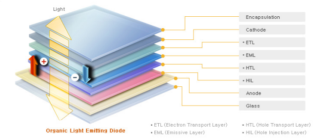
7.1 OLED照明スタック 7-3
8.1 VTED蒸着システムの概略図 8-4
8.2 OVPDD蒸着システムの概略図 8-7
8.3 VTEとOVPD技術の比較 8-9
8.4 インクジェット蒸着システムの概略図 8-10
8.5 R2RD蒸着システムの概略図 8-12
8.6 OLED上の平坦化層の図 8-25
9.1 PMOLEDの概略図 9-2
9.2 PMOLEDスタック/駆動アーキテクチャ 9-3
9.3 AMOLEDの概略図 9-5
9.4 パッシブマトリックスOLEDの容量と需要 9-8
9.5 アクティブマトリックスOLEDの容量と需要 9-10
10.1 LEDの分野別市場 10-24
10.2 世界のLED市場予測 10-25

Summary
The High Brightness Light Emitting Diode (HB LED) market is exploding as unit shipments continue their upward growth. LEDs are creating a niche market for conventional suppliers of semiconductor processing tools. Markets for HB LEDs, backlight LEDs, and OLEDs are forecast.
In the rapidly evolving landscape of lighting technology, LED (Light Emitting Diode) and OLED(Organic Light Emitting Diode) lighting stand at the forefront, heralding a new era of efficiency,sustainability, and design flexibility. The "LED and OLED Lighting: Market Analysis and Manufacturing Trends" report offers an in-depth exploration of these two pivotal technologies,providing a comprehensive overview of their current market status, growth trajectories, and the technological innovations that drive them.
As the global push towards energy efficiency and reduced carbon footprints intensifies, LED and OLED lighting solutions have emerged as pivotal players. Their unique attributes—notably, their energy efficiency, longer lifespans, and superior light quality—have propelled them into the spotlight, not just as alternatives to traditional lighting solutions, but as the preferred choice in a wide range of applications,from residential and commercial to industrial and architectural.
This report begins by dissecting the market dynamics of the LED and OLED sectors, analyzing key growth drivers, challenges, and opportunities. It delves into the regulatory frameworks and environmental mandates across different regions that have been instrumental in shaping the market landscape, highlighting how policy shifts are influencing demand patterns and technological advancements.
Technological innovation remains at the heart of LED and OLED development, with ongoing research and development efforts pushing the boundaries of what's possible in lighting technology. The report examines the latest advancements in material science, including novel phosphors and organic materials, that are enhancing the performance and efficiency of LED and OLED lights. It also explores the evolution of design trends, from the miniaturization of components to the integration of smart technology, which are expanding the applications and appeal of these lighting solutions.
The manufacturing landscape for LED and OLED technologies is also a focal point of this report.It assesses the impact of global supply chains, the role of economies of scale, and the strategic moves by leading manufacturers as they navigate the complexities of production, from cost considerations to the adoption of sustainable manufacturing practices.
Furthermore, the report provides a detailed analysis of the competitive environment,identifying key players, their market positioning, and strategies for innovation and growth. It also offers insights into the emerging markets and sectors that represent growth opportunities for LED and OLED technologies, including automotive lighting, horticultural applications, and wearable electronics.
Looking ahead, the report forecasts the future directions of the LED and OLED markets,considering factors such as potential technological breakthroughs, emerging economic trends,and shifts in consumer preferences. It identifies challenges that could impede growth, such as material shortages or competitive pressures, and opportunities that could fuel expansion, such as the increasing demand for smart and connected lighting systems.
In conclusion, the "LED and OLED Lighting: Market Analysis and Manufacturing Trends" report serves as an essential resource for stakeholders across the lighting industry spectrum, offering strategic insights and actionable intelligence to navigate the complexities of the market,leverage emerging opportunities, and shape the future of lighting technology.
Trends in LED and OLED Lighting
The lighting industry is undergoing a significant transformation, driven by the rapid advancements and adoption of LED (Light Emitting Diode) and OLED (Organic Light Emitting Diode) technologies. These shifts are not only changing the way spaces are illuminated but also how lighting solutions are designed, manufactured, and integrated into the modern digital ecosystem. The key trends shaping the LED and OLED lighting markets include:
About This Report
The comprehensive report "LED and OLED Lighting: Market Analysis and Manufacturing Trends"offers an in-depth exploration of the LED and OLED lighting sectors, aiming to provide a comprehensive overview of market dynamics and manufacturing trends.
It begins by providing an in-depth overview of the current market size and growth trajectory,shedding light on key factors driving market expansion, such as increasing demand for energyefficient lighting solutions, advancements in lighting technologies, and growing consumer awareness regarding environmental sustainability.
Furthermore, the report explores the latest technological innovations and trends in LED and OLED lighting, including advancements in efficiency, color rendering capabilities, and integration with smart lighting systems. It examines emerging trends such as miniaturization,flexible lighting solutions, and the integration of Internet of Things (IoT) technologies into lighting systems, offering insights into their impact on market dynamics.
Moreover, the report delves into the intricacies of LED and OLED lighting manufacturing processes, detailing key manufacturing techniques, materials, and equipment utilized in the production of LED and OLED lighting products. It examines supply chain dynamics, including raw material sourcing, manufacturing partnerships, and distribution channels, providing a comprehensive understanding of the industry's operational ecosystem.
Additionally, the report assesses regulatory landscapes governing the LED and OLED lighting industries, including energy efficiency standards, environmental regulations, and safety certifications. It also conducts a competitive analysis, profiling leading players in the market and evaluating their strategies, product portfolios, and market positioning.
Furthermore, the report offers detailed market segmentation analysis, categorizing the LED and OLED lighting market based on factors such as product type, application, end-user industry, and geographic region. It provides insights into market trends and growth opportunities across various segments, enabling stakeholders to identify lucrative investment opportunities and devise effective business strategies.
Finally, the report presents a forward-looking outlook for the LED and OLED lighting market,forecasting future growth prospects, emerging market trends, and potential challenges. It equips industry stakeholders, including manufacturers, investors, policymakers, and industry professionals, with actionable insights to make informed decisions and stay ahead in a rapidly evolving market landscape.
Table of ContentsChapter1 Introduction 1-1Chapter 2 Recent Progress in High Brightness LED Technology and Applications 2-1
2.1 LED:Theoryof Operation 2-1
2.2 Intellectual Property Map 2-5
2.3 LEDManufacturing Technologies&Costs 2-7
2.4 LEDMarket General Illumination 2-13
Chapter3 Processing Equipment 3-1
3.1 Introduction 3-1
3.2 Deposition 3-3
3.2.1 MOCVDfor SSL– Productivity Challengesand Solutions 3-3
3.2.2 Low temperature Remote Plasma Chemical Vapor Deposition(RPCVD)3-12
3.3 Chemical Mechanical Planarization 3-15
3.4 Defect Inspectionand Testing 3-20
3.5 Lithography 3-24
3.5.1 Steppers 3-24
Chapter4 Materialsof Construction 4-1
4.1 Introduction 4-1
4.2 Ga N-based LEDfor General Lighting 4-7
4.2.1 Methodsto Improve White LEDEfficiency 4-18
4.2.2 Time-to-Marketfor LEDsubstrates 4-20
4.3 LEDPhosphor Manufacturing Issues 4-21
4.3.1 Current LEDPhosphor Manufacturing 4-21
4.3.2 LEDPhosphor Cost 4-23
Chapter5 Packagingand Assembly Issuesfor High Brightness LEDs 5-1
5.1 Packagingfor HBLEDs 5-1
5.1.1 Bonding 5-5
5.1.2 Die/Ball Bonding 5-9
5.1.3 Scribing 5-12
5.2 Wafer Level Packaging HBLEDs 5-15
5.3 Thermal Issues 5-21
5.4 Testand Inspection 5-24
Chapter6 National Programs As Innovation Drivers 6-1
6.1 DOESolid-State Lighting Manufacturing Initiative 6-1
6.2 DOESolid-State Lighting Program Missionand Goal 6-1
6.3 Major National Research Programs Pertainingto LEDs 6-4
6.4 Challenges Facing SSLManufacturing 6-9
Chapter7 OLEDLighting 7-1
7.1 Opportunitiesfor Luminaire Manufacturers 7-1
7.2 How Doesan OLEDWork 7-1
7.3 Differences Between OLEDLightingand OLEDDisplay 7-4
7.4 Benefitsof OLEDLighting Technology 7-6
7.5 OLEDPerformance Metrics 7-7
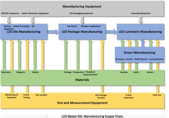
Chapter8 OLEDManufacturing 8-1
8.1 Deposition Equipmentand Processesfor OLEDLighting 8-1
8.1.1 Vacuum Deposition Or Vacuum Thermal Evaporation(VTE) 8-3
8.1.2 Organic Vapor Deposition(OVPD) 8-6
8.1.3 Inkjet Printing 8-8
8.1.4 Roll-to-Roll(R2R) 8-11
8.2 General OLEDManufacturing Cost Considerations 8-13
8.3 Lithography 8-16
8.4 Substratesand Encapsulation 8-17
8.4.1 Substrateand Encapsulation Material Selection 8-18
8.4.2 Substrate Coatings 8-19
8.4.3 Transparent Electrodes 8-20
8.4.4 Encapsulation 8-22
8.5 Inspectionand Quality Control 8-24
Chapter9 Outlookforthe Worldwide OLEDMarket 9-1
9.1 Introduction 9-1
9.2 Passive Matrix Capacityand Demand 9-6
9.3 Active Matrix Capacityand Demand 9-9
9.4 Cost Challengesfor OLEDLighting 9-11
Chapter10 Outlookforthe Worldwide High-Brightness LEDMarket 10-1
10.1 HBLEDTechnology 10-1
10.2 HBLEDMarket Overviewandtrends 10-4
10.2.1 Market Driversfor SSL 10-7
10.2.2 LEDBacklightsfor Notebook PCs 10-8
10.2.3 LEDBacklightsfor LCDTVs 10-10
10.2.4 LEDBacklightsfor Other Applications 10-12
10.2.5 LEDLighting Market 10-14
10.2.6 LEDActive Outdoor Display Market 10-16
10.2.7 LEDSignal Market 10-18
10.2.8 LEDAutomotive Market 10-20
10.2.9 LEDMobile Market 10-22
List of Tables/GraphsListof Tables
2.1 Color,Wavelength Material Of LED 2-3
2.2 Light Source Comparison 2-21
2.3 Comparisonof LED,HB-LED,UHB-LEDCharacteristics 2-23
3.1 Epitaxy Metricsfrom Initial Solid-State Lighting Manufacturing R&DRoadmap 3-5
3.2 Process Control Metrics 3-16
4.1 Production Methodfor Various LEDs 4-3
4.2 LEDCost Model:Impactof Substrate Choice 4-14
4.3 Comparisonof$/klmfor LEDMadeon Various2"Substrates 4-15
5.1 Propertiesof Die Bonding Processes 5-6
7.1 Efficiencyof Emitter Materials 7-9
7.2 Statusof Technology Towards Lighting Targets 7-11
7.3 Cost Targetsfor Panels 7-13
7.4 Cost Comparison OLEDDisplayvs Lighting 7-14
8.1 Cost Targetsfor Panels Producedby Traditional Methods 8-15
10.1 Forecastof LEDBacklightsfor Notebook PCs 10-9
10.2 Forecastof LEDBacklightsfor LCDTVs 10-11
10.3 Forecastof LEDBacklightsfor Other Application 10-13
10.4 Forecastof LEDLighting Market 10-15
10.5 Forecastof LEDActive Outdoor Display Market 10-17
10.6 Forecastof LEDSignal Market 10-19
10.7 Forecastof LEDAutomotive Market 10-21
10.8 Forecastof LEDMobile Market 10-23
10.9 Top10LEDVendors 10-26
Listof Figures
2.1 Operationof LED 2-2
2.2 Key Intellectual Property Relationships 2-6
2.3 DOERoadmap 2-8
2.4 Relative Manufacturing Costs 2-10
2.5 Pareto Analysis Of SSLManufacturing Costs 2-12
2.6 Marketdriversfor LEDBizand Applications 2-14
2.7 SSLvs.Classical Technologies 2-15
2.8 LEDPerformancevs.Traditional Light Sources 2-16
2.9 Energy Productionand Use Comparison 2-18
2.10 Worldwide LEDMarket Forecast 2-20
3.1 SSL– LEDmanufacturingwith MOCVD:productivity and Cost Analysis 3-6
3.2 Larger Wafer Size:Ga NLEDs 3-7
3.3 Global Shipmentsof MOCVDTools By Vendor 3-10
3.4 Global Shipmentsof MOCVDTools By Region 3-11
3.5 Diagramof RPCVDReactor 3-13
3.6 Comparisonbetween MOCVDand RPCVD 3-14
3.7 CMPProcess 3-16
3.8 Nanoimprint Lithography System 3-26
3.9 The Phlatlight Chip 3-30
4.1 Regular LED(white)Front-End Steps 4-5
4.2 Current Blocking Layer 4-6
4.3 Regular LED(white)Production Costsfor100kwafers/year 4-12
4.4 HBLED(white)Production Costsfor100kwafers/year 4-13
4.5 Main Manufacturing Stepsfor Ga N-based LED 4-16
4.6 Regular LED(white)Back-End 4-17
4.7 Methodsto Improve White LEDEfficiency 4-19
4.8 Phosphor Coating– Four Approaches 4-24
5.1 Hybrid Integration Approachto HD-LEDPackage 5-3
5.2 Chain Wire Bond 5-11
5.3 HB-LEDwith Silicon Carrier Submount 5-17
5.4 Siliconinterposerfor MEMS/LEDApplications 5-18
5.5 High Brightness LED 5-19
5.6 SMDPackage Cost Structure 5-20
5.7 Packaging Changes Resultin Optical Improvements 5-22
5.8 Substrate Solutionsfor HB/HPLEDs 5-23
6.1 DOESolid-State Lighting Program Strategy 6-2
6.2 DOEEfficacy Targets 6-3
6.3 Congressional Appropriations 6-6
6.4 SSLR&DProject Funding 6-7
6.5 Price Targets 6-8
7.1 OLEDLighting Stack 7-3
8.1 Schematicof VTEDeposition System 8-4
8.2 Schematicof OVPDDeposition System 8-7
8.3 Comparison Between VTEand OVPDTechnology 8-9
8.4 Schematicof Inkjet Deposition System 8-10
8.5 Schematicof R2RDeposition System 8-12
8.6 Illustrationof Planarization Layeron OLED 8-25
9.1 Schematicof PMOLED 9-2
9.2 PMOLEDStack/Driving Architecture 9-3
9.3 Schematicof AMOLED 9-5
9.4 Passive Matrix OLEDCapacityand Demand 9-8
9.5 Active Matrix OLEDCapacityand Demand 9-10
10.1 LEDMarketby Sector 10-24
10.2 Worldwide LEDMarket Forecast 10-25
ご注文は、お電話またはWEBから承ります。お見積もりの作成もお気軽にご相談ください。本レポートと同分野(電子部品/半導体)の最新刊レポート
The Information Network社の 半導体プロセスレポートシリーズ分野 での最新刊レポートよくあるご質問The Information Network社はどのような調査会社ですか?インフォメーションネットワーク (The Information Network) は、半導体製造に関連する材料や半導体のエンドアプリケーションなどの市場を幅広く調査・分析する米国ペンシルベニア州の調... もっと見る 調査レポートの納品までの日数はどの程度ですか?在庫のあるものは速納となりますが、平均的には 3-4日と見て下さい。
注文の手続きはどのようになっていますか?1)お客様からの御問い合わせをいただきます。
お支払方法の方法はどのようになっていますか?納品と同時にデータリソース社よりお客様へ請求書(必要に応じて納品書も)を発送いたします。
データリソース社はどのような会社ですか?当社は、世界各国の主要調査会社・レポート出版社と提携し、世界各国の市場調査レポートや技術動向レポートなどを日本国内の企業・公官庁及び教育研究機関に提供しております。
|
|


.png)