フリップチップ/ウェハレベルパッケージ(WLP)製造と市場分析Flip Chip/WLP Manufacturing and Market Analysis フリップチップは、携帯電話、デジタルカメラ、MP3プレーヤー、コンピュータ周辺機器など、多様な高ボリューム消費者製品に広く採用されています。本報告書では、フリップチップICの市場をデバイスアプリケー... もっと見る

サマリー
フリップチップは、携帯電話、デジタルカメラ、MP3プレーヤー、コンピュータ周辺機器など、多様な高ボリューム消費者製品に広く採用されています。本報告書では、フリップチップICの市場をデバイスアプリケーション別に分析し、その製造に用いられるリソグラフィーとウェットエッチングツールについても考察しています。
はじめに
半導体業界は、電子デバイスの性能、信頼性、小型化を向上させるパッケージング技術の進歩に牽引され、絶え間なく進化を続けている。これらの技術の中でも、フリップチップとウエハーレベルパッケージング(WLP)は、次世代半導体デバイスの重要な実現要素として浮上してきた。これらのパッケージング技術は、小型化、高機能化、電気的性能の向上という点で比類のない利点を提供し、現代の電子システムに不可欠なものとなっている。半導体フリップチップおよびWLP市場は、
家電、自動車、ヘルスケア、通信など様々な最終用途産業における小型で高性能な電子機器への需要の高まりに後押しされ、
近年著しい成長を遂げている。
小型化、高機能化、高信頼性への要求がますます高まる中、フリップチップ技術とWLP技術は、こうした課題に対応するための不可欠なソリューションとなっています。
半導体フリップチップとWLPに関するこの包括的なレポートは、業界の軌道を形成する主要トレンド、推進要因、課題、機会を含む市場環境の詳細な分析を提供します。本レポートは、技術的進歩、市場ダイナミクス、競争環境に焦点を当て、関係者が十分な情報に基づいた意思決定を行い、新たな市場動向を活用するための貴重な洞察を提供することを目的としています。
本レポートの主な内容は以下の通りです:
市場概要:市場規模、成長促進要因、業界の課題など、半導体フリップチップとWLP市場の詳細な概要。現在の市場状況を調査し、予測期間における市場成長と採用動向の予測を提供しています。
技術展望:フリップチップとWLP技術について、その原理、製造プロセス、主要な進歩などを包括的に分析。ファンアウトウェーハレベルパッケージング(FOWLP)、シリコン貫通ビア(TSV)、 、ヘテロジニアスインテグレーションなどの新たなトレンドについて調査し、半導体パッケージングエコシステムへの影響を強調しています。
アプリケーションインサイト:民生用電子機器、車載用電子機器、ヘルスケア機器、通信インフラなど、さまざまな業界でフリップチップとWLP技術の採用を促進する主要なアプリケーション分野を検証。各アプリケーション分野の成長機会と市場動向を明らかにしています。
競合分析:主要企業のプロフィール、製品ポートフォリオ、主要戦略、最近の動向など、競争環境の詳細な評価を掲載しています。半導体フリップチップおよびWLP市場の主要企業が採用している市場ポジショニング、競争力、潜在的成長戦略に関する洞察を提供します。
市場の展望と機会:半導体フリップチップとWLP市場の市場動向、新たなビジネスチャンス、今後の成長見通しについて展望的に分析します。市場機会を活用し、潜在的なリスクを軽減するための戦略的提言を関係者に提供します。
半導体フリップチップ/WLP(ウェーハレベルパッケージング)の動向
ペースの速い半導体製造の世界では、技術革新が進歩の原動力となっています。無数の進歩の中で、フリップチップとウェーハレベルパッケージング(WLP)は、電子デバイスの状況を一変させる極めて重要な技術として浮上してきた。小型化、高性能化、高機能化に焦点を当てたこれらのパッケージング技術は、半導体部品の集積方法を再構築し、小型で高性能なエレクトロニクスの新時代への道を開いている。この記事では、半導体フリップチップ/WLP市場を形成する最新トレンドを掘り下げ、このダイナミックな業界を前進させる主要なドライバー、イノベーション、機会を探る。
市場の成長と拡大
半導体フリップチップ/WLP市場は、さまざまな産業でより小型で高性能な電子機器への需要が高まっていることを背景に、力強い成長を遂げています。製造プロセスと材料技術の進歩に伴い、フリップチップとWLPソリューションは、スマートフォンやウェアラブルから車載エレクトロニクスやIoTデバイスに至るまで、幅広いアプリケーションで採用されるようになってきている。最新の電子システムの進化するニーズに対応するため、メーカーが革新的なパッケージング・ソリューションを求めていることから、市場はさらに拡大する態勢を整えている。
技術の進歩:
フリップチップとWLPの進歩の中心は技術革新である。市場を形成している主要トレンドの1つは、ファンアウト・ウェハーレベル・パッケージング(FOWLP)の採用であり、コスト効率、小型化、電気性能の向上という点で大きなメリットがある。さらに、シリコン貫通ビア(TSV)は3D集積の重要な実現要因として台頭し、半導体デバイスの集積密度と性能の向上を可能にしている。その他の注目すべき動向には、異種集積技術の開発や、シリコンフォトニクスや窒化ガリウム(GaN)などの先端材料のパッケージングプロセスへの統合が含まれる。

アプリケーションの多様化:
フリップチップとWLP技術は、多様な産業で応用されており、特定の最終用途の要件に合わせた特殊なパッケージング・ソリューションの需要を促進している。民生用電子機器分野では、フリップチップ/WLPソリューションが、より小型でエネルギー効率に優れ、機能が強化されたデバイスの開発を促進している。自動車業界では、これらの技術によって先進運転支援システム(ADAS)、インフォテインメント・システム、V2X(Vehicle-to-Everything)通信モジュールの統合が可能になっています。さらに、ヘルスケアと通信の分野では、フリップチップ/WLPソリューションが次世代医療機器、ネットワークインフラ、5G対応機器の開発で重要な役割を果たしている。
市場ダイナミクスと競争環境:
半導体フリップチップ/WLP市場は、激しい競争と急速な技術進歩が特徴である。業界をリードするプレーヤーは、時代の先端を走り、競争力を得るために研究開発に多額の投資を行っています。さらに、戦略的パートナーシップ、合併、買収が競争環境を形成し、統合を促進し、技術革新を促進している。市場が進化を続ける中、半導体メーカー、パッケージング企業、装置サプライヤー間の協力は、新たな機会を引き出し成長を促進する上で極めて重要である。
将来の展望と機会:
将来を展望すると、半導体フリップチップ/WLP市場の将来は有望であり、イノベーションと成長のチャンスは十分にある。パッケージング技術の継続的な進歩と、人工知能(AI)、モノのインターネット(IoT)、車載エレクトロニクスなどの新興アプリケーションの普及が相まって、フリップチップおよびWLPソリューションの需要が促進されると予想される。さらに、半導体デバイスがますます複雑化、異種化するにつれて、高度なパッケージング・ソリューションへのニーズは高まる一方であり、市場プレーヤーに新たなビジネスチャンスをもたらしている。
本レポートについて
この半導体フリップチップ/WLP(ウェーハレベルパッケージング)レポートは、半導体業界の様々なステークホルダーにとって貴重な洞察と戦略的優位性を提供します。本レポートを購入するメリットとして、以下の点が挙げられます。
市場分析:包括的なレポートでは、市場規模、成長傾向、フリップチップ/WLP市場を形成する主要な要因など、現在の市場環境に関する詳細な分析を提供しています。この情報は、ステークホルダーが市場の動向を理解し、成長機会を特定するのに役立ちます。
競合情報:本レポートは、主要企業のプロファイル、市場シェア、戦略的取り組みなど、競争環境に関する洞察を提供します。これらの情報を活用することで、企業は競合他社と自社のパフォーマンスを比較し、競争優位性を獲得するための効果的な戦略を策定することができます。
技術トレンド:半導体フリップチップ/WLP技術は急速に進化しており、新たなイノベーションと進歩が定期的に生まれています。本レポートでは、パッケージング技術、材料、製造プロセスの進歩など、最新の技術トレンドを詳細に分析しています。これらの知識は、企業が常に時代の先を行き、最先端技術を導入してイノベーションを推進する上で役立ちます。
業界洞察:本レポートは、フリップチップ/WLPソリューションの需要を牽引する様々なアプリケーションとエンドユーザー業界に関する貴重な洞察を提供します。各業界が直面する固有の要件と課題を理解することで、企業は顧客ニーズに効果的に対応した製品とサービスを開発することができます。
投資機会:投資家や金融機関にとって、半導体フリップチップ/WLPレポートは、市場における投資機会に関する貴重な情報を提供します。
市場動向、成長見通し、競争動向を分析することで、投資家は情報に基づいた意思決定を行い、戦略的に資本を配分することができます。
目次第1章はじめに 第2章エグゼクティブサマリー第3章フリップチップ/WLPの課題と動向
3.1はじめに
3.2ウェーハバンピング
3.2.1はんだバンプ
3.2.1.1冶金学
3.2.1.2UBMの析出
3.2.1.3スパッタエッチング
3.2.1.4フォトリソグラフィ
3.2.1.5はんだ析出
3.2.1.6レジストストリップ
3.2.1.7UBMウェットエッチング
3.2.1.8リフロー
3.2.1.9フラックスの問題
3.2.2金バンプ
3.2.1バンプ処理
3.2.2接合
3.2.2.3コプラナリティ
3.2.2.4導電率
3.2.2.5熱特性
3.2.2.6サイズ
3.2.2.7信頼性
3.2.2.8コスト問題
3.2.3銅柱バンプ
3.2.4銅スタッドバンプ
3.2.5C4NP
3.3ウェハレベルパッケージング
3.4パッド再分配
3.5ウェハバンプコスト
3.5.1ウェハ再分配とウェハバンプコスト
3.5.2WLCSPの隠れたコスト
3.5.3WLCSPの良品ダイあたりのコスト
3.5.4ウェハレベルアンダーフィルコスト
3.6パネルレベルパッケージング
第4章リソグラフィの課題と動向
4.1課題
4.1.1技術性能
4.1.2設備投資
4.1.3消耗品コスト
4.1.4スループット
4.1.5使いやすさ
4.1.6柔軟性
4.1.7装置サポート
4.1.8解像度
4.1.9はんだバンピング能力
4.1.10金バンピング能力
4.2露光装置
4.2.1紹介
4.2.1.1リダクションステッパー
4.2.1.2フルフィールドプロジェクション
4.2.1.3マスクアライナー
4.2.1.41Xステッパー
4.2.1.52Xステッパー
4.3競合技術
4.3.1インクジェット印刷
4.3.2ステンシル/スクリーン印刷
4.3.3無電解金属蒸着
第5章UBMエッチングの課題と動向
5.1はじめに
5.2技術の課題と動向
5.2.1プロセスフロー
5.2.2エッチングプロセス
5.2.3エッチング化学
5.3バッチ対枚葉エッチング
第6章メタライゼーションの課題と動向
6.1はじめに
6.2スパッタリングメタライゼーション
6.2.1金バンプ
6.2.2はんだバンプ
6.2.1T I / CuおよびTiW / Cu
6.2.2Al / NiV / Cu
6.2.3T i / N i (V)およびTiW / Ni ( V )
6.2.2.4Cr / Cr--Cu / Cu
6.2.3銅バンプ
6.3電解めっき
第7章市場分析
7.1フリップチップとWLPの市場促進要因
7.2市場機会
7.3課題
7.4フリップチップ市場
7.4.1市場ダイナミクス
7.4.2市場予測
7.5リソグラフィ市場
7.5.1アライナー対ステッパー
7.5.2市場分析
7.6蒸着市場
図表リスト図表
3.1はんだおよび金バンピング用の一般的なUBMスタック
3.2はんだバンピングガイドライン
3.3金バンピングガイドライン
3.4銅バンピングガイドライン
3.5はんだバンピングプロセスの比較
3.6アプリケーション別のITRSピン数
3.7Pillar-WLP CSPガイドライン
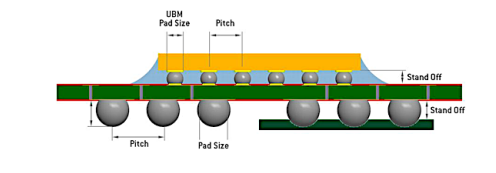
3.8パッド再配分ガイドライン
4.1WLPリソグラフィの主な課題
4.2ベンダー別リソグラフィツール
5.1UBM膜エッチャント
5.2スピンプロセスの利点
6.1金とはんだバンピング用の一般的なUBMスタック
7.1デバイス別WLP需要(ユニット)
7.2デバイス別WLP需要(ウェハ)
7.3世界リソグラフィ予測
7.41xステッパーと2xステッパーの所有コスト
7.5成膜ツールの世界予測
図のリスト
3.1C4チップの接続
3.2ウェーハバンプ技術のロードマップ
3.3銅柱、フリップチップ、WLPの比較
3.4はんだバンピングプロセス
3.5はんだバンプの3つのプロセスフロー
3.6金バンププロセス
3.7金バンプウェハあたりのコスト
3.8銅スタッドバンプ
3.9スタッドバンプコストの内訳
3.1C4NPプロセスの説明
3.11ピラー-WLPCSPプロセス
3.12パッド再配布プロセス
4.1レーザー・プロジェクション・イメージング
4.2はんだジェット技術

Summary
Flip chips are appearing in a plethora of high-volume consumer products such as mobile phones, digital cameras, MP3 players, and computer peripherals. This report examines the market for flip chip ICs by device application, and the lithography and wet etch tools used in their manufacture
Introduction
The semiconductor industry is continually evolving, driven by advancements in packaging technologies that enhance performance, reliability, and miniaturization of electronic devices. Among these technologies, Flip Chip and Wafer-Level Packaging (WLP) have emerged as critical enablers of next-generation semiconductor devices. These packaging techniques offer unparalleled advantages in terms of size reduction, increased functionality, and improved electrical performance, making them indispensable in modern electronic systems. The semiconductor Flip Chip and WLP market have witnessed significant growth in recent years,
fueled by the growing demand for compact, high-performance electronic devices across various end-use industries such as consumer electronics, automotive, healthcare, and telecommunications. As manufacturers strive to meet the ever-increasing demands for smaller form factors, higher functionality, and greater reliability, Flip Chip and WLP technologies have become essential solutions for addressing these challenges.
This comprehensive report on semiconductor Flip Chip and WLP provides a detailed analysis of the market landscape, including key trends, drivers, challenges, and opportunities shaping the industry's trajectory. With a focus on technological advancements, market dynamics, and competitive landscape, this report aims to provide stakeholders with valuable insights to make informed decisions and capitalize on emerging market trends.
Key components of the report include:
Market Overview: An in-depth overview of the semiconductor Flip Chip and WLP market,including market size, growth drivers, and industry challenges. The report examines the current market landscape and provides forecasts for market growth and adoption trends over the forecast period.
Technology Landscape: A comprehensive analysis of Flip Chip and WLP technologies, including their principles, manufacturing processes, and key advancements. The report explores emerging trends such as fan-out wafer-level packaging (FOWLP), through-silicon vias (TSVs), and heterogeneous integration, highlighting their impact on the semiconductor packaging ecosystem.
Application Insights: An examination of key application areas driving the adoption of Flip Chip and WLP technologies across various industries, including consumer electronics, automotive electronics, healthcare devices, and telecommunications infrastructure. The report identifies growth opportunities and market trends in each application segment.
Competitive Analysis: A detailed assessment of the competitive landscape, including the profiles of leading players, their product portfolios, key strategies, and recent developments.The report provides insights into market positioning, competitive strengths, and potential growth strategies adopted by key players in the semiconductor Flip Chip and WLP market.
Market Outlook and Opportunities: A forward-looking analysis of market trends, emerging opportunities, and future growth prospects in the semiconductor Flip Chip and WLP market. The report offers strategic recommendations for stakeholders to capitalize on market opportunities and mitigate potential risks.
Trends in Semiconductor Flip Chip/WLP (Wafer Level Packaging)
In the fast-paced world of semiconductor manufacturing, innovation drives progress. Among the myriad of advancements, Flip Chip and Wafer-Level Packaging (WLP) have emerged as pivotal technologies revolutionizing the landscape of electronic devices. With a focus on size reduction, enhanced performance, and increased functionality, these packaging techniques are reshaping the way semiconductor components are integrated, paving the way for a new era of compact, high-performance electronics. In this article, we delve into the latest trends shaping the semiconductor Flip Chip/WLP market, exploring the key drivers, innovations, and opportunities propelling this dynamic industry forward.
Market Growth and Expansion:
The semiconductor Flip Chip/WLP market is experiencing robust growth, driven by the escalating demand for smaller, more powerful electronic devices across a multitude of industries. With advancements in manufacturing processes and material technologies, Flip Chip and WLP solutions are increasingly being adopted in applications ranging from smartphones and wearables to automotive electronics and IoT devices. The market is poised for further expansion as manufacturers seek innovative packaging solutions to meet the evolving needs of modern electronic systems.
Technological Advancements:
Technological innovation lies at the heart of Flip Chip and WLP advancements. One of the key trends shaping the market is the adoption of fan-out wafer-level packaging (FOWLP), which offers significant advantages in terms of cost efficiency, miniaturization, and improved electrical performance. Additionally, through-silicon vias (TSVs) have emerged as a critical enabler of 3D integration, allowing for greater integration density and enhanced performance in semiconductor devices. Other notable trends include the development of heterogeneous integration techniques and the integration of advanced materials such as silicon photonics and gallium nitride (GaN) into packaging processes.
Application Diversification:
Flip Chip and WLP technologies are finding applications across a diverse range of industries,driving demand for specialized packaging solutions tailored to specific end-use requirements. In the consumer electronics sector, Flip Chip/WLP solutions are facilitating the development of smaller, more energy-efficient devices with enhanced functionality. In the automotive industry,these technologies are enabling the integration of advanced driver-assistance systems (ADAS),infotainment systems, and vehicle-to-everything (V2X) communication modules. Moreover, in the healthcare and telecommunications sectors, Flip Chip/WLP solutions are playing a crucial role in the development of next-generation medical devices, network infrastructure, and 5Genabled devices.
Market Dynamics and Competitive Landscape:
The semiconductor Flip Chip/WLP market is characterized by intense competition and rapid technological advancements. Leading players in the industry are investing heavily in research and development to stay ahead of the curve and gain a competitive edge. Moreover, strategic partnerships, mergers, and acquisitions are shaping the competitive landscape, driving consolidation and fostering innovation. As the market continues to evolve, collaboration between semiconductor manufacturers, packaging companies, and equipment suppliers will be crucial to unlocking new opportunities and driving growth.
Future Outlook and Opportunities:
Looking ahead, the future of the semiconductor Flip Chip/WLP market looks promising, with ample opportunities for innovation and growth. Continued advancements in packaging technologies, coupled with the proliferation of emerging applications such as artificial intelligence (AI), Internet of Things (IoT), and automotive electronics, are expected to drive demand for Flip Chip and WLP solutions. Moreover, as semiconductor devices become increasingly complex and heterogeneous, the need for advanced packaging solutions will only continue to grow, presenting new opportunities for market players to capitalize on.
About This Report
This semiconductor flip chip/WLP (wafer level packaging) report can provide invaluable insights and strategic advantages for various stakeholders within the semiconductor industry. Here are several compelling reasons why purchasing such a report could be beneficial:
Market Analysis: A comprehensive report offers a detailed analysis of the current market landscape, including market size, growth trends, and key drivers shaping the flip chip/WLP market. This information can help stakeholders understand the market dynamics and identify growth opportunities.
Competitive Intelligence: The report provides insights into the competitive landscape, including profiles of key players, their market share, and strategic initiatives. This information enables companies to benchmark their performance against competitors and devise effective strategies to gain a competitive edge.
Technology Trends: Semiconductor flip chip/WLP technology is rapidly evolving, with new innovations and advancements emerging regularly. A detailed report delves into the latest technology trends, including advancements in packaging techniques, materials, and manufacturing processes. This knowledge can help companies stay ahead of the curve and adopt cutting-edge technologies to drive innovation.
Industry Insights: The report offers valuable insights into the various applications and end-user industries driving demand for flip chip/WLP solutions. Understanding the specific requirements and challenges faced by different industries allows companies to tailor their products and services to meet customer needs effectively.
Investment Opportunities: For investors and financial institutions, a semiconductor flip chip/WLP report provides valuable information on investment opportunities within the market.
By analyzing market trends, growth prospects, and competitive dynamics, investors can make informed decisions and allocate capital strategically.
Table of ContentsChapter1 IntroductionChapter2 Executive SummaryChapter3 Flip Chip/WLP Issues and Trends
3.1 Introduction
3.2 Wafer Bumping
3.2.1 Solder Bumps
3.2.1.1 Metallurgy
3.2.1.2 Deposition Of UBM
3.2.1.3 Sputter Etching
3.2.1.4 Photolithography
3.2.1.5 Solder Deposition
3.2.1.6 Resist Strip
3.2.1.7 UBM Wet Etch
3.2.1.8 Reflow
3.2.1.9 Flux Issues
3.2.2 Gold Bumps
3.2.2.1 Bump Processing
3.2.2.2 Bonding
3.2.2.3 Coplanarity
3.2.2.4 Conductivity
3.2.2.5 Thermal Properties
3.2.2.6 Size
3.2.2.7 Reliability
3.2.2.8 Cost Issues
3.2.3 Copper Pillar Bumps
3.2.4 Copper Stud Bumping
3.2.5 C4NP
3.3 Wafer Level Packaging
3.4 Pad Redistribution
3.5 Wafer Bumping Costs
3.5.1 Wafer Redistribution And Wafer Bumping Costs
3.5.2 WLCSP Hidden Costs
3.5.3 WLCSP Cost Per Good Die
3.5.4 Wafer-‐Level Underfill Costs
3.6 Panel Level Packaging
Chapter 4Lithography Issues And Trends
4.1 Issues
4.1.1 Technical Performance
4.1.2 Capital Investment
4.1.3 Cost Of Consumables
4.1.4 Throughput
4.1.5 Ease Of Use
4.1.6 Flexibility
4.1.7 Equipment Support
4.1.8 Resolution
4.1.9 Solder Bumping Capabilities
4.1.10 Gold Bumping Capabilities
4.2 Exposure Systems
4.2.1 Introduction
4.2.1.1 Reduction Steppers
4.2.1.2 Full-‐Field Projection
4.2.1.3 Mask Aligners
4.2.1.4 1X Steppers
4.2.1.5 2X Steppers
4.3 Competitive Technologies
4.3.1 Inkjet Printing
4.3.2 Stencil/Screen Printing
4.3.3 Electroless Metal Deposition
Chapter 5UBM Etch Issues And Trends
5.1 Introduction
5.2 Technology Issues And Trends
5.2.1 Process Flow
5.2.2 Etch Process
5.2.3 Etch Chemistry
5.3 Batch Versus Single-‐Wafer Etching
Chapter 6Metallization Issues and Trends
6.1 Introduction
6.2 Sputtering Metallization
6.2.1 Gold Bump
6.2.2 Solder Bumping
6.2.2.1 T I / Cu and TiW / Cu
6.2.2.2 Al / NiV / Cu
6.2.2.3 T i / N i (V) and TiW / Ni ( V )
6.2.2.4 Cr / Cr-‐Cu / Cu
6.2.3 Copper Bumping
6.3 Electrodeposition
Chapter 7Market Analysis
7.1 Market Drivers For Flip Chip And WLP
7.2 Market Opportunities
7.3 Challenges
7.4 Flip Chip Market
7.4.1 Market Dynamics
7.4.2 Market Forecast
7.5 Lithography Market
7.5.1 Aligners Vs. Steppers
7.5.2 Market Analysis
7.6 Deposition Market
List of Tables/GraphsList of Tables
3.1 Common UBM Stacks For Solder And Gold Bumping
3.2 Solder Bumping Guidelines
3.3 Gold Bumping Guidelines
3.4 Copper Bumping Guidelines
3.5 Comparison Of Solder Bumping Processes
3.6 ITRS Pin Counts For Different Applications
3.7 Pillar-WLP CSP Guidelines
3.8 Pad Redistribution Guidelines
4.1 Key Challenges For WLP Lithography
4.2 Lithography Tools By Vendor
5.1 UBM Film Etchants
5.2 Advantages Of Spin Processing
6.1 Common UBM Stacks For Gold And Solder Bumping
7.1 WLP Demand by Device (Units)
7.2 WLP Demand by Device (Wafers)
7.3 Worldwide Lithography Forecast
7.4 Cost Of Ownership Of 1x Versus 2x Steppers
7.5 Worldwide Forecast For Deposition Tools
List of Figures
3.1 C4 Chip Connections
3.2 Wafer Bump Technology Roadmap
3.3 Comparison Of Copper Pillar, Flip Chip, And WLP
3.4 Solder Bumping Process
3.5 Three Process Flows For Solder Bumping
3.6 Gold Bumping Process
3.7 Cost Per Gold Bumped Wafer
3.8 Copper Stud Bump
3.9 Breakdown Of Stud Bumping Costs
3.1 C4NP Process Description
3.1 1Pillar-WLPCSP Process
3.1 2Pad Redistribution Process
4.1 Laser-Projection Imaging
4.2 Solder Jet Technology
ご注文は、お電話またはWEBから承ります。お見積もりの作成もお気軽にご相談ください。本レポートと同分野(電子部品/半導体)の最新刊レポート
The Information Network社の 半導体プロセスレポートシリーズ分野 での最新刊レポートよくあるご質問The Information Network社はどのような調査会社ですか?インフォメーションネットワーク (The Information Network) は、半導体製造に関連する材料や半導体のエンドアプリケーションなどの市場を幅広く調査・分析する米国ペンシルベニア州の調... もっと見る 調査レポートの納品までの日数はどの程度ですか?在庫のあるものは速納となりますが、平均的には 3-4日と見て下さい。
注文の手続きはどのようになっていますか?1)お客様からの御問い合わせをいただきます。
お支払方法の方法はどのようになっていますか?納品と同時にデータリソース社よりお客様へ請求書(必要に応じて納品書も)を発送いたします。
データリソース社はどのような会社ですか?当社は、世界各国の主要調査会社・レポート出版社と提携し、世界各国の市場調査レポートや技術動向レポートなどを日本国内の企業・公官庁及び教育研究機関に提供しております。
|
|

