薄膜蒸着:動向、重要課題、市場分析Thin Film Deposition: Trends, Key Issues, Market Analysis 本レポートでは、技術動向、製品、用途、材料・機器のサプライヤーについて論じている。また、将来のユーザーニーズに対するサプライヤーの洞察も提供し、長期計画、新製品開発、製品改良の一助となるはずです... もっと見る

サマリー
本レポートでは、技術動向、製品、用途、材料・機器のサプライヤーについて論じている。また、将来のユーザーニーズに対するサプライヤーの洞察も提供し、長期計画、新製品開発、製品改良の一助となるはずです。PVD、LPCVD、PECVD、SACVD、HDPCVD、MOCVD、ALD向け薄膜成膜装置の市場予測を掲載しています。各分野の市場シェアも掲載。
はじめに
半導体業界では、薄膜蒸着は電子デバイスの製造 プロセスにおいて重要な役割を担っており、 半導体基板上に薄膜材料を精密かつ制御しながら蒸着する方法を提供している。 半導体薄膜蒸着市場を形成している注目すべきトレンドはいくつかあり、技術の進歩、 産業要件の進化、新たなアプリケーションを反映している。
第一に、高い スループット、均一性、スケーラビリティを提供する薄膜蒸着技術に対する需要が高まっている。半導体デバイスがますます複雑化し、集積化されるにつれて、メーカーは、より大きな基板サイズに対応し、全表面積にわたって一貫した膜特性を実現できる成膜方法を必要としている。この傾向は、原子層堆積法(ALD)や化学気相成長法(CVD)などの革新的な成膜プロセスの開発を促しており、大量生産を可能にしながら、膜厚や組成を正確に制御することができる。
半導体薄膜成膜市場のもう一つの傾向は、薄膜成膜に先端材料を採用する傾向が強まっていることである。デバイスの性能要求が高まるにつれ、
導電性、光学的透明性、熱安定性の向上など、特性を調整した薄膜へのニーズが高まっている。この傾向は、次世代電子デバイスの進化する要求を満たすための新材料の探求に焦点を当てた研究開発の努力を後押ししている。
さらに、3次元(3D)半導体構造や異種集積プラットフォームの製造をサポートする薄膜成膜技術への注目も高まっている。3D ICやシステムオンチップ(SoC)アーキテクチャーのような技術の出現により、非平面上に薄膜を成膜し、正確な層間アライメントを達成できる成膜手法に対するニーズが高まっている。
さらに、薄膜成膜技術をin situモニタリングおよび制御機能と統合し、リアルタイムのプロセス最適化と欠陥検出を可能にする傾向もある。先進の計測ツールとフィードバック機構を成膜システムに組み込むことで、メーカーはプロセスの安定性、歩留まり、再現性を高め、半導体デバイスの生産コストと市場投入までの時間を削減することができる。
全体として、半導体薄膜成膜市場の動向は、優れた性能、機能性、信頼性を備えた高度な電子デバイスの製造を可能にする革新的なソリューションに対する業界の継続的な探求を浮き彫りにしている。半導体技術が進化し続ける中、薄膜蒸着は半導体産業の進歩と革新を推進する重要な実現技術であり続けるだろう。
成膜技術の動向
半導体薄膜成膜技術の動向は、高精度化、材料の多様化、デバイスの複雑化、環境の持続可能性、プロセスのインテリジェント化といった動きを特徴としている。これらの傾向は、新しい成膜方法と材料の開発を形成し、前例のない性能と機能を備えた次世代の電子デバイスに向けて半導体産業を牽引している。
半導体薄膜成膜技術の状況は、電子デバイスの小型化、性能の向上、コスト効率のあくなき追求によって、大きな変貌を遂げつつある。この進化は、半導体業界の要求の変化と、これらのニーズを満たすために設計された技術革新を反映するいくつかの重要な傾向によって特徴づけられる。
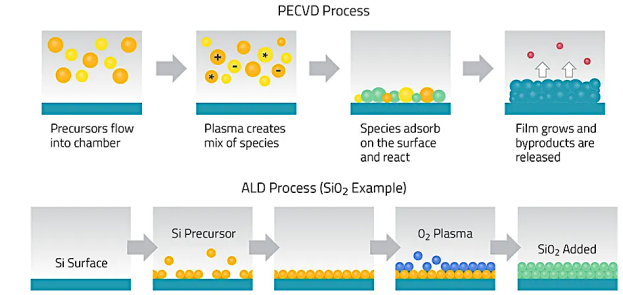
極めて重要なトレンドは、薄膜形成プロセスにおける原子レベルの精密さへのシフトである。原子層蒸着(ALD)のような技術は、一度に1原子層ずつ成膜する能力で脚光を浴びており、膜厚と組成を比類なく制御できる。この精度は、わずかなずれでもデバイスの性能に大きな影響を与える次世代半導体デバイスの製造に不可欠である。複雑な3次元構造をコンフォーマルにコーティングできるALDの能力は、3次元集積回路(IC)や高度なメモリー技術を含む高度なアプリケーションに不可欠である。
もうひとつの重要なトレンドは、薄膜形成に使用される材料の多様化である。従来のシリコンをベースとする半導体は、高誘電率、金属酸化物、グラフェンや遷移金属ジカルコゲナイドのような二次元(2D)材料など、さまざまな新しい材料によって補強されたり、置き換えられたりしている。これらの材料は優れた電気的、熱的、機械的特性を持ち、より高性能で低消費電力のデバイスの開発を可能にする。これらの材料を取り入れるには、そのユニークな特性と統合の課題に対応できる成膜技術の進歩が必要である。
デバイスの高集積化と高機能化の推進により、複雑な多層構造の採用が進んでおり、厳密な層間界面と均一性を備えた高品質の膜を提供できる高度な成膜技術が必要とされています。デバイスの微細化と層数の増加に伴い、成膜技術は、デバイスの信頼性と性能を確保するために、界面工学、応力管理、層の均一性に関して優れた制御を提供する必要があります。
環境の持続可能性とエネルギー効率もまた、薄膜成膜プロセスにおいて重要な考慮事項となってきている。半導体業界は、製造プロセスにおける環境フットプリントの削減にますます注力しており、より少ないエネルギーを消費し、より少ない有害化学物質を使用し、より少ない廃棄物を発生させる成膜技術の開発につながっている。この傾向は、規制の圧力だけでなく、長期的な存続のために持続可能な慣行が重要であるという業界の認識にも後押しされている。
最後に、成膜プロセスへのin-situモニタリングと分析の統合は、増加傾向にある。高度なセンサーとデータ分析が蒸着システムに直接組み込まれ、リアルタイムのプロセス制御と最適化を可能にしている。この統合により、プロセスの再現性が向上し、歩留まりが改善され、成膜後の検査の必要性が減るため、製造コストの削減とデバイス性能の向上が可能になる。
本レポートの必要性
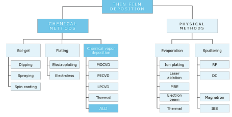
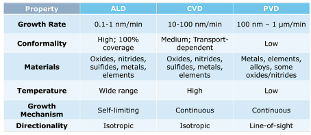
この包括的な半導体成膜レポートは、半導体製造に極めて重要な成膜技術の多面的な領域を深く掘り下げています。本レポートは、薄膜成膜の基礎的な概要から始まり、物理的気相成長法(PVD)、化学的気相成長法(CVD)、原子層堆積法(ALD)、分子線エピタキシー法(MBE)などの重要なプロセスに光を当てています。このセクションでは、各手法の背後にある原理を解明し、独自の利点、限界、さまざまな半導体アプリケーションへの適合性を理解するのに役立つ比較分析を提供します。
市場ダイナミクスについては、世界および地域の動向を詳細に調査し、市場の成長、需要パターン、将来予測を明らかにしています。本レポートでは、競争環境について包括的な図を描き、主要企業の特定、市場での位置づけ、戦略的イニシアティブ、技術的ブレークスルーを紹介しています。さらに、規制の枠組みや環境基準が成膜作業に与える影響についても論じており、持続可能性と安全性の義務付けに対する業界の対応を強調している。
本レポートでは技術の進歩が中心的な役割を果たし、膜質、成膜効率、材料の多様性を高める最新の技術革新を紹介している。2D材料、高誘電率誘電体、金属酸化物など、半導体デバイスの性能に革命をもたらす新材料の登場を強調している。また、これらの先進的な成膜プロセスを主流製造に統合する際の課題にも言及し、スケーラビリティ、品質管理、費用対効果にも言及している。
最先端の電子デバイスの製造における蒸着技術の応用を徹底的に分析している。これには、ロジックチップ、メモリーデバイス、パワーエレクトロニクスの開発における役割や、3D集積回路(IC)、フレキシブルエレクトロニクス、太陽電池などの新興分野への貢献が含まれる。本レポートは将来を展望し、既存の技術的ハードルの克服、プロセス能力の向上、環境に優しい成膜方法の発見を目指した研究開発の方向性を推測している。
結論として、本レポートは成膜技術の展望を示し、研究の優先課題、解決が待たれる技術的課題、予想される市場の変化を明らかにしている。また、ケーススタディや専門家の意見を掲載し、実際の事例や権威ある洞察に基づいた予測を行うことで、読者に半導体成膜技術の現状と将来の可能性を包括的に理解してもらう。
本レポートは、メーカーや研究者から政策立案者や投資家に至るまで、半導体業界の関係者にとって貴重な情報源となり、急速な技術変化の時代における半導体成膜の複雑さを乗り切るための知識を提供する。
本レポートについて
薄膜蒸着プロセスは、高密度で高性能なマイクロエレクトロニクス製品の生産において重要な役割を担っている。成膜プロセスの開発と、それを行うリアクターシステムの開発において、かなりの進歩が達成されている。本報告書では、関連するメカニズム、プロセス、システム、材料の側面、潜在的な進歩、ウェーハ直径300mmおよびそれ以上への拡張性に関する考察について述べる。
一貫して縮小を続けるマイクロエレクトロニクスデバイスや回路に新しい薄膜材料が導入され、集積回路構造の開口率が増大するにつれて、コンフォーマルステップカバレッジの達成はますます困難になっている。本レポートでは、以下のようなさまざまな成膜ツールのユーザーに影響を与える問題のいくつかを比較している:
さらに、デバイス形状の微細化に伴い、半導体製造はますます複雑かつ精密になっており、関連する特定のプロセスについてより深い理解が必要となっている。本レポートでは、このような問題について解説する。
本レポートでは、技術動向、製品、アプリケーション、材料や装置のサプライヤーについて論じている。また、将来のユーザーニーズに対するサプライヤーへの洞察も与えており、長期計画、新製品開発、製品改良の一助となるはずである。
2012年から2023年までの成膜タイプ別市場シェアを含む、薄膜成膜ツールの市場予測を掲載しています。
目次Chapter 1 はじめにChapter 2 エグゼクティブサマリー 2-1Chapter 3 Physical Vapor Deposition 3-1
3.1 はじめに 3-1
3.2 スパッタリング技術 3-2
3.3 プラズマ技術 3-5
3.4 リアクター設計 3-14
3.4.1 ロングスロー蒸着 3-14
3.4.2 Collimated Sputter Deposition 3-16
3.4.3 Showerhead Deposition 3-18
3.4.4 Ionized PVD 3-22
3.5 Semiconductor Processing 3-28
3.5.1 Feature Patterning 3-28
3.5.2 Gap Fill 3-31
3.6 Targets 3-34
Chapter 4 Chemical Vapor Deposition 4-1
4.1 はじめに 4-1
4.2 化学的気相成長(CVD)技術 4-1
4.2.1 APCVD 4-1
4.2.2 LPCVD 4-6
4.2.3 PECVD 4-9
4.2.4 HDPCVD 4-13
4.2.5 ALD 4-19
第5章 電気化学的蒸着 5-1
5.1 はじめに 5-1
5.2 リアクターの設計 5-5
5.3 課題 5-6
5.4 添加剤 5-8
5.5 処理 5-9
5.5.1 スーパーフィリング 5-9
5.5.2 アスペクト比 5-9
5.6 銅カソード 5-10
5.7 ウェット銅シード層 5-11
第6章 成膜と膜特性 6-1
6.1 はじめに 6-1
6.2 誘電体蒸着 6-4
6.2.1 二酸化ケイ素 6-5
6.2.1.1 熱CVD 6-5
6.2.1.2 PECVD6-6
6.2.1.3 HDPCVD 6-9
6.2.2 窒化ケイ素 6-13
6.2.2.1 熱CVD 6-13
6.2.2.2 PECVD6-14
6.2.2.3 HDPCVD 6-19
6.2.3 高誘電率絶縁膜 6-19
6.2.4 低誘電率絶縁膜 6-22
6.3 金属蒸着 6-23
6.3.1 アルミニウム 6-23
6.3.2 タングステン/ケイ化タングステン 6-26
6.3.3 窒化チタン 6-28
第7章 ベンダー問題 7-1
7.1 はじめに 7-1
7.2 450mm加工 7-6
7.3 集積加工 7-8
7.4 銅 7-11
7.5 測定 7-14
7.6 ESD 7-17
7.7 パラメトリック・テスト 7-18
第8章 市場予測 8-1
8.1 はじめに 8-1
8.2 主要課題 8-4
8.3 市場予測の前提 8-7
8.4 市場予測 8-8
8.4.1 化学蒸着 8-8
8.4.2 物理蒸着 8-28
8.4.3 銅電気めっき市場 8-32
8.4.4 原子層蒸着市場 8-36
図表リスト図リスト
3.1 スパッタリングシステムの概略図 3-3
3.2 マグネトロンスパッタリング設計 3-9
3.3 シャワーヘッドリアクター設計 3-19
3.4 イオン化PVD 3-24
4.1 APCVDリアクター 4-3
4.2 チューブ CVD リアクター 4-7
4.3 HDPCVD リアクター 4-17
4.4 ALD 対 PVD 銅バリア 4-26
5.1 銅電気めっきシステム 5-3
7.1 半導体と装置収益の比較 7-4
8.1 MCVDの世界市場シェア 8-12
8.2 DCVDの世界市場シェア 8-13
8.3 DCVDの世界市場(セクター別) 8-15
8.4 HDHCVDの世界市場シェア 8-18
8.5 PECVDの世界市場シェア 8-21
8.6 SACVDの世界市場シェア 8-24
8.7 LPCVDの世界市場シェア 8-27
8.8 PVDの世界市場シェア 8-31
8.9 世界の ECD 市場シェア 8-34
8.10 世界の ALD 市場シェア 8-38
表の一覧
8.1 世界の CVD 市場予測 8-9
8.2 世界の MCVD 市場シェア 8-10
8.3 Worldwide DCVD Market Shares 8-11
8.4 Worldwide HDPCVD Market Forecast 8-16
8.5 Worldwide HDPCVD Market Shares 8-17
8.6 Worldwide PECVD Market Forecast 8-19
8.7 世界の PECVD 市場シェア 8-20
8.8 世界の SACVD 市場予測 8-22
8.9 世界の SACVD 市場シェア 8-23
8.10 世界の LPCVD 市場予測 8-25
8.11 世界の LPCVD 市場シェア 8-26
8.12 世界の PVD 市場予測 8-29
8.13 世界の PVD 市場シェア 8-30
8.14 世界の ECD 市場予測 8-33
8.15 世界の ALD 市場予測 8-37

Summary
This report discusses the technology trends, products, applications, and suppliers of materials and equipment. It also gives insight to suppliers for future user needs and should assist them in long range planning, new product development and product improvement. A market forecast for Thin Film Deposition Tools for PVD, LPCVD, PECVD, SACVD, HDPCVD, MOCVD, ALD, is presented. Market shares for each of these sectors is presented.
Introduction
In the semiconductor industry, thin film deposition plays a crucial role in the manufacturing process of electronic devices, providing a method to deposit thin layers of materials onto semiconductor substrates with precision and control. Several notable trends are shaping the semiconductor thin film deposition markets, reflecting advancements in technology, evolving industry requirements, and emerging applications.
Firstly, there is a growing demand for thin film deposition techniques that offer high throughput, uniformity, and scalability. As semiconductor devices become increasingly complex and integrated, manufacturers require deposition methods that can accommodate larger substrate sizes and deliver consistent film properties across the entire surface area. This trend is driving the development of innovative deposition processes, such as atomic layer deposition (ALD) and chemical vapor deposition (CVD), which offer precise control over film thickness and composition while enabling high-volume production.
Another trend in the semiconductor thin film deposition markets is the increasing adoption of advanced materials for thin film deposition. As device performance requirements continue to escalate, there is a
growing need for thin films with tailored properties, such as enhanced electrical conductivity, optical transparency, and thermal stability. This trend is driving research and development efforts focused on exploring new materials to meet the evolving demands of next-generation electronic devices.
Furthermore, there is a rising emphasis on thin film deposition techniques that support the fabrication of three-dimensional (3D) semiconductor structures and heterogeneous integration platforms. With the advent of technologies like 3D ICs and system-on-chip (SoC) architectures, there is a growing need for deposition methods capable of depositing thin films on non-planar surfaces and achieving precise layer-to layer alignment.
Moreover, there is a trend towards the integration of thin film deposition techniques with in situ monitoring and control capabilities, enabling real-time process optimization and defect detection. By incorporating advanced metrology tools and feedback mechanisms into deposition systems, manufacturers can enhance process stability, yield, and reproducibility, thereby reducing production costs and time-to-market for semiconductor devices.
Overall, the trends in the semiconductor thin film deposition markets underscore the industry's ongoing quest for innovative solutions that enable the fabrication of advanced electronic devices with superior performance, functionality, and reliability. As semiconductor technologies continue to evolve, thin film deposition will remain a critical enabling technology, driving progress and innovation in the semiconductor industry.
Trends in Deposition Technology
The trends in semiconductor thin film deposition technology are characterized by a move towards greater precision, material diversity, device complexity, environmental sustainability, and process intelligence. These trends are shaping the development of new deposition methods and materials, driving the semiconductor industry towards the next generation of electronic devices with unprecedented performance and functionality.
The landscape of semiconductor thin film deposition technology is undergoing significant transformation, driven by the relentless pursuit of miniaturization, enhanced performance, and cost-efficiency in electronic devices. This evolution is marked by several key trends that reflect the changing demands of the semiconductor industry and the technological innovations designed to meet these needs.
A pivotal trend is the shift towards atomic precision in thin film deposition processes. Techniques such as Atomic Layer Deposition (ALD) are gaining prominence for their ability to deposit films one atomic layer at a time, offering unparalleled control over film thickness and composition. This precision is crucial for manufacturing the next generation of semiconductor devices, where even minor deviations can significantly impact device performance. ALD's ability to conformally coat complex 3D structures makes it indispensable for advanced applications, including 3D integrated circuits (ICs) and advanced memory technologies.
Another significant trend is the diversification of materials used in thin film deposition. Traditional silicon-based semiconductors are being augmented or replaced by a variety of new materials, including high-k dielectrics, metal oxides, and two-dimensional (2D) materials like graphene and transition metal dichalcogenides. These materials offer superior electrical, thermal, and mechanical properties, enabling the development of devices with higher performance and lower power consumption. The incorporation of these materials necessitates advancements in deposition technologies that can handle their unique properties and integration challenges.
The push for greater device integration and functionality is driving the adoption of complex multi-layer structures, which require sophisticated deposition techniques capable of delivering high-quality films with strict interlayer interfaces and uniformity. As devices shrink and the number of layers increases, deposition technologies must offer excellent control over interface engineering, stress management, and layer uniformity to ensure device reliability and performance.
Environmental sustainability and energy efficiency are also becoming critical considerations in thin film deposition processes. The semiconductor industry is increasingly focused on reducing the environmental footprint of manufacturing processes, leading to the development of deposition techniques that consume less energy, use fewer hazardous chemicals, and generate less waste. This trend is not only driven by regulatory pressures but also by the industry's recognition of the importance of sustainable practices for long-term viability.
Lastly, the integration of in-situ monitoring and analytics with deposition processes is a growing trend. Advanced sensors and data analytics are being incorporated directly into deposition systems, enabling real-time process control and optimization. This integration enhances process repeatability, improves yield, and reduces the need for post-deposition inspection, thereby lowering manufacturing costs and improving device performance.
The Need for This Report
This comprehensive semiconductor deposition report provides an in-depth exploration into the multifaceted domain of deposition technologies pivotal to semiconductor manufacturing. It begins with a foundational overview of thin film deposition, shedding light on critical processes such as physical vapor deposition (PVD), chemical vapor deposition (CVD), atomic layer deposition (ALD), and molecular beam epitaxy (MBE). This section demystifies the principles behind each method, offering a comparative analysis to aid in understanding their unique benefits, limitations, and suitability for various semiconductor applications.
Delving into market dynamics, the report presents a detailed examination of global and regional trends, highlighting market growth, demand patterns, and future projections. It paints a comprehensive picture of the competitive landscape, identifying key players, their market positioning, strategic initiatives, and technological breakthroughs. Furthermore, it discusses the impact of regulatory frameworks and environmental standards on deposition practices, emphasizing the industry's response to sustainability and safety mandates.
Technological advancements occupy a central role in the report, showcasing the latest innovations that enhance film quality, deposition efficiency, and material diversity. It highlights the advent of new materials like 2D materials, high-k dielectrics, and metal oxides that promise to revolutionize semiconductor device performance. The narrative extends to the challenges of integrating these advanced deposition processes into mainstream manufacturing, addressing scalability, quality control, and cost-effectiveness.
The application of deposition technologies in fabricating cutting-edge electronic devices is thoroughly analyzed. This includes their role in developing logic chips, memory devices, power electronics, and their contribution to emerging sectors like 3D integrated circuits (ICs), flexible electronics, and solar cells. The report ventures into the future, speculating on the direction of research and development efforts aimed at overcoming existing technological hurdles, enhancing process capabilities, and discovering
environmentally friendly deposition methods.
In its concluding sections, the report provides a forward-looking perspective on the deposition technology landscape, identifying research priorities, technological challenges awaiting resolution, and anticipated market shifts. It features case studies and expert opinions to ground its predictions in real-world examples and authoritative insights, offering readers a well rounded understanding of the current state and future potential of semiconductor deposition technologies.
By weaving together these diverse strands of information, the report serves as a valuable resource for stakeholders across the semiconductor industry spectrum, from manufacturers and researchers to policymakers and investors, equipping them with the knowledge to navigate the complexities of semiconductor deposition in an era of rapid technological change.
About this Report
Thin film deposition processes play a critical role in the production of high-density, high performance microelectronic products. Considerable progress has been achieved in the development of deposition processes -- and in the development of the reactor systems in which they are carried out. This report discusses relevant mechanisms; processing, system, and materials aspects, potential advances, and considerations regarding extendibility to a wafer diameter of 300 mm and beyond.
With the introduction of new thin-film materials to consistently shrinking microelectronic devices and circuits, and as the aperture ratio of an integrated-circuit structure increases, conformal step coverage becomes increasingly difficult to achieve. This report compares some of the issues impacting users of different deposition tools, including:
In addition, as device geometries shrink, semiconductor manufacturing has become increasingly complex and precise, requiring a better understanding of the specific processes involved. These issues are described in the report.
This report discusses the technology trends, products, applications, and suppliers of materials and equipment. It also gives insights to suppliers for future user needs and should assist them in long range planning, new product development and product improvement. A market forecast for Thin Film Deposition
Tools is presented including market shares by deposition type between 2012 and 2023.
Table of ContentsChapter 1 Introduction 1-1Chapter 2 Executive Summary 2-1Chapter 3 Physical Vapor Deposition 3-1
3.1 Introduction 3-1
3.2 Sputtering Technology 3-2
3.3 Plasma Technology 3-5
3.4 Reactor Designs 3-14
3.4.1 Long-Throw Deposition 3-14
3.4.2 Collimated Sputter Deposition 3-16
3.4.3 Showerhead Deposition 3-18
3.4.4 Ionized PVD 3-22
3.5 Semiconductor Processing 3-28
3.5.1 Feature Patterning 3-28
3.5.2 Gap Fill 3-31
3.6 Targets 3-34
Chapter 4 Chemical Vapor Deposition 4-1
4.1 Introduction 4-1
4.2 Chemical Vapor Deposition (CVD) Techniques 4-1
4.2.1 APCVD 4-1
4.2.2 LPCVD 4-6
4.2.3 PECVD 4-9
4.2.4 HDPCVD 4-13
4.2.5 ALD 4-19
Chapter 5 Electrochemical Deposition 5-1
5.1 Introduction 5-1
5.2 Reactor Design 5-5
5.3 Challenges 5-6
5.4 Additives 5-8
5.5 Processing 5-9
5.5.1 Superfilling 5-9
5.5.2 Aspect Ratios 5-9
5.6 Copper Cathodes 5-10
5.7 Wet Copper Seed-Layer 5-11
Chapter 6 Film Deposition And Film Properties 6-1
6.1 Introduction 6-1
6.2 Dielectric Deposition 6-4
6.2.1 Silicon Dioxide 6-5
6.2.1.1 Thermal CVD 6-5
6.2.1.2 PECVD 6-6
6.2.1.3 HDPCVD 6-9
6.2.2 Silicon Nitride 6-13
6.2.2.1 Thermal CVD 6-13
6.2.2.2 PECVD 6-14
6.2.2.3 HDPCVD 6-19
6.2.3 High-K Dielectrics 6-19
6.2.4 Low-K Dielectrics 6-22
6.3 Metal Deposition 6-23
6.3.1 Aluminum 6-23
6.3.2 Tungsten/Tungsten Silicide 6-26
6.3.3 Titanium Nitride 6-28
Chapter 7 Vendor Issues 7-1
7.1 Introduction 7-1
7.2 450mm Processing 7-6
7.3 Integrated Processing 7-8
7.4 Copper 7-11
7.5 Metrology 7-14
7.6 ESD 7-17
7.7 Parametric Test 7-18
Chapter 8 Market Forecast 8-1
8.1 Introduction 8-1
8.2 Key Issues 8-4
8.3 Market Forecast Assumptions 8-7
8.4 Market Forecast 8-8
8.4.1 Chemical Vapor Deposition 8-8
8.4.2 Physical Vapor Deposition 8-28
8.4.3 Copper Electroplating Market 8-32
8.4.4 Atomic Layer Deposition Market 8-36
List of Tables/GraphsList of Figures
3.1 Schematic Of Sputtering System 3-3
3.2 Magnetron Sputtering Design 3-9
3.3 Showerhead Reactor Design 3-19
3.4 Ionized PVD 3-24
4.1 APCVD Reactor 4-3
4.2 Tube CVD Reactor 4-7
4.3 HDPCVD Reactor 4-17
4.4 ALD Versus PVD Copper Barrier 4-26
5.1 Copper Electroplating System 5-3
7.1 Comparison Between Semiconductor and Equipment Revenues 7-4
8.1 Worldwide MCVD Market Shares 8-12
8.2 Worldwide DCVD Market Shares 8-13
8.3 Worldwide DCVD Market By Sectors 8-15
8.4 Worldwide HDHCVD Market Shares 8-18
8.5 Worldwide PECVD Market Shares 8-21
8.6 Worldwide SACVD Market Shares 8-24
8.7 Worldwide LPCVD Market Shares 8-27
8.8 Worldwide PVD Market Shares 8-31
8.9 Worldwide ECD Market Shares 8-34
8.10 Worldwide ALD Market Shares 8-38
List of Tables
8.1 Worldwide CVD Market Forecast 8-9
8.2 Worldwide MCVD Market Shares 8-10
8.3 Worldwide DCVD Market Shares 8-11
8.4 Worldwide HDPCVD Market Forecast 8-16
8.5 Worldwide HDPCVD Market Shares 8-17
8.6 Worldwide PECVD Market Forecast 8-19
8.7 Worldwide PECVD Market Shares 8-20
8.8 Worldwide SACVD Market Forecast 8-22
8.9 Worldwide SACVD Market Shares 8-23
8.10 Worldwide LPCVD Market Forecast 8-25
8.11 Worldwide LPCVD Market Shares 8-26
8.12 Worldwide PVD Market Forecast 8-29
8.13 Worldwide PVD Market Shares 8-30
8.14 Worldwide ECD Market Forecast 8-33
8.15 Worldwide ALD Market Forecast 8-37
ご注文は、お電話またはWEBから承ります。お見積もりの作成もお気軽にご相談ください。本レポートと同分野(前工程装置)の最新刊レポート
The Information Network社の 半導体プロセスレポートシリーズ分野 での最新刊レポートよくあるご質問The Information Network社はどのような調査会社ですか?インフォメーションネットワーク (The Information Network) は、半導体製造に関連する材料や半導体のエンドアプリケーションなどの市場を幅広く調査・分析する米国ペンシルベニア州の調... もっと見る 調査レポートの納品までの日数はどの程度ですか?在庫のあるものは速納となりますが、平均的には 3-4日と見て下さい。
注文の手続きはどのようになっていますか?1)お客様からの御問い合わせをいただきます。
お支払方法の方法はどのようになっていますか?納品と同時にデータリソース社よりお客様へ請求書(必要に応じて納品書も)を発送いたします。
データリソース社はどのような会社ですか?当社は、世界各国の主要調査会社・レポート出版社と提携し、世界各国の市場調査レポートや技術動向レポートなどを日本国内の企業・公官庁及び教育研究機関に提供しております。
|
|