世界各国のリアルタイムなデータ・インテリジェンスで皆様をお手伝い
Global Semiconductor Equipment: Markets, Market Shares and Market Forecasts世界の半導体製造装置:市場、市場シェア、市場予測 This report describes the semiconductor equipment markets for more than 24 different sectors and profiles 43 leading equipment companies in the U.S., Europe, and Asia. Market shares for each com... もっと見る
本レポートは毎月更新を行っています。最新情報はお気軽にお問合せください。 

Summary
This report describes the semiconductor equipment markets for more than 24 different sectors and profiles 43 leading equipment companies in the U.S., Europe, and Asia. Market shares for each company for each sector are presented, and each sector is forecast.
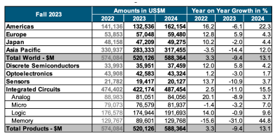
The Semiconductor Industry Association (SIA) announced global semiconductor industry sales totaled $526.8 billion in 2023, a decrease of 8.2% compared to the 2022 total of $574.1 billion, which was the industry’s highest-ever annual total. Sales picked up during the second half of 2023. In fact, fourth-quarter sales of $146.0 billion were 11.6% more than the total from the fourth quarter of 2022 and 8.4% higher than the total from third quarter of 2023. And global sales for the month of December 2023 were $48.6 billion, an increase of 1.5% compared to November 2023 total. Monthly sales are compiled by the World Semiconductor Trade Statistics (WSTS) organization and represent a three-month moving average. SIA represents 99% of the U.S. semiconductor industry by revenue and nearly two-thirds of non-U.S. chip firms.
On a regional basis, Europe was the only regional market that experienced annual growth in 2023, with sales there increasing 4.0%. Annual sales into all other regional markets decreased in 2023: Japan (-3.1%), the Americas (-5.2%), AsiaPacific/All Other (-10.1%), and China (-14.0%). Sales for the month of December 2023 increased compared to November 2023 in China (4.7%), the Americas (1.8%), and Asia Pacific/All Other (0.3%), but decreased in Japan (-2.4%) and Europe (-3.9%).
Several semiconductor product segments stood out in 2023. Sales of logic products totaled $178.5 billion in 2023, making it the largest product category by sales.Memory products were second in terms of sales, totaling $92.3 billion. Microcontroller units (MCUs) grew by 11.4% to a total of $27.9 billion. And sales of automotive ICs grew by 23.7% year-over-year to a record total of $42.2 billion.
Global economic slowdowns and capes overspend were catalysts for producing an oversupply of semiconductors and an equipment meltdown in 2023. A significant capacity expansion is underway as current fabs expand and new fabs are planned.
A push by the Biden administration to invest $50 billion on domestic manufacturing facilities to improve US self-sufficiency and reduce reliance on Asia has initiated a course that will likely result in oversupply and capacity expansion:
Intel
• Arizona – Fab 42 expansion for 7nm capacity
• Oregon – Fab D1X $3B Mod3 expansion; tools installed Aug. ‘21 to Feb. ‘22
• New Mexico - $3.5B spend for advanced packaging
• Israel - $10B 7nm fab; 2023 production
• Ireland – spent additional $7B from 2019-2021 to expand to 7nm
• Arizona Foundry $20B for 2 fabs (~35k wspm each) starting production in 2023 and 2024
• Malaysia – $7B for advanced packaging fab expansion; 2024 production
TSMC
• Fab 18 – 3nm $20B fab expected to be completed in 2023
• Arizona Fab –$12B over time; 5nm initial phase to produce 20k wspm starting in 1Q24 with equipment installation commencing in
2H2022
• Japan 22 / 28nm fab with Sony; $7B 45k wspm targeting late 2024 production
• 7/6nm & 28nm fab in Kaohsiung, Taiwan for 2024 production for a reported $10B; phase 1 = 40k wspm for 7nm and 6nm with phase
2 for 28nm
Samsung
• Pyeongtaek line 3 (P3) equipment move-in expected to start in April 2022; rst 40-50k wspm 176L 3D NAND line, 130k-140k wspm
DRAM and 10k-20k wspm 5nm foundry lines in 2H2022
• Pyeongtaek P2 S5-1; 3nm 60k wspm in 2021 & ramp to 120k wspm in 2022
• Pyeongtaek P2 S5-2; 3nm 60k wspm targeted production in 2024
• U.S. $17B 5nm Foundry fab in Texas; expected 2H2024 production (120k wspm est.)
GlobalFoundries
• $4 billion Singapore Module 7H 38k wspm starting wafer production in early-2023; full ramp end of 2023
• $1B Malta New York fab expansion of 12,500 wspm; additional fab to double capacity
• Spending $1.4B to expand capacity in U.S., Singapore, and Germany
SMIC
• 100k wspm 28nm & above fab for $8.87B in Shanghai; timing unknown
• 40k wspm 28nm & above fab in Shenzhen for $2.35B; production starting 2022
UMC
• Fab 12A Phase 6 (P6) $3.5B plan for expansion; scheduled for production in 2Q23
Kioxia / Western Digital
• Fab 7 in Mie Prefecture, Japan; expected production in late 2022 / early 2023
• Kitakami (K2) fab at $18.4B expected completion in early 2023; use of Yokkaichi equip.?
Micron• DRAM - $7B fab in Japan expected to commence production in 2024 SK Hynix
• $106B fab complex with 800k wspm capacity and 200k EUV – rst fab completed in 2025
Nanya
• DRAM - $10.7B 10nm 110k wspm fab expected to be completed in 2023; production in 2024
Powerchip Semi (PSMC)
• $10B 12-inch fab in the Tongluo Science Park; 100k wspm of 1x to 50nm technology will be put into production in stages beginning in
2023
Texas Instruments
• RFAB2 - $850M fab coming online in 2H2022 with equipment over next few years
• LFAB (acquired from Micron) – spend $3B of capex over time with target of coming online in early-2023 – more details in February at
capital management call
• North Texas Fab site (option for up to 4 fabs over time) – 1st & 2nd fab construction commencing in 2022 with First fab targeting
production in 2025 (70k wspm estimated)
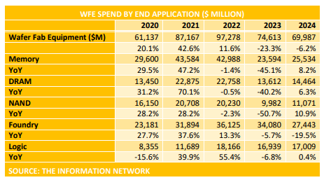
Wafer Front End equipment spend between 2020 and 2024 by device end product is shown below
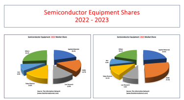
In Figure 1.1 below, we show market shares for the global WFE equipment market for 2022 and 2023, listing shares for the Top 5 global equipment companies and the other equipment companies in the market.
 Industry Trends
The increased use of semiconductors has been accompanied by an increase in their complexity. Due to the creation of new applications and markets for semiconductors, suppliers and manufacturers are faced with an increasing demand for new products that provide greater functionality and higher performance at lower prices. As a result, many new complex materials, structures and processes are being introduced into semiconductor manufacturing ecosystem.
Such materials include, among others, copper, low-k and high-k dielectrics, silicon-on-insulator, silicon-germanium, III-V, strained silicon and raised source/drain.Manufacturers have transitioned in the past years toward 300 mm silicon wafers (from 200 mm silicon wafers). While 300 mm wafers can yield up to twice as many integrated circuits than 200 mm wafers, they also create new manufacturing challenges. For example, because 300 mm wafers can bend or bow more than twice than the 200 mm wafers, they are more susceptible to damage. The larger area of 300 mm wafers also makes it more difficult to maintain film uniformity across the entire wafer.
Semiconductors also continue to move toward smaller feature sizes and more complex structures such as 3D FinFET transistors, GAA (Gate All Around), 3D-NAND and emerging memory structures. The growing complexity of semiconductor devices increase the complexity and the costs of the semiconductor manufacturing process,which has also been a driver for the growing demand for metrology systems.
The ever-increasing level of complexity and the decrease in feature sizes has also significantly increased the cost and performance requirements of semiconductor fabrication equipment. The cost of wafer fabrication equipment has also increased due to the higher levels of automation being utilized by manufacturers. Thus,semiconductor manufacturers must increase their investment in capital equipment in
order to sustain technological leadership, to expand manufacturing capacity and maintain profitability.
Many of the manufacturing steps involve the controlled application or removal of layers of materials to or from the wafer. The application of materials to the wafer,known as deposition, involves the layering of extremely thin films of electrically insulating, conducting or semi-conducting materials. These layers can range from onethousandth to less than one-hundred-thousandth of a millimeter in thickness and create electrically active regions on the wafer and its surface.
A wide range of materials and deposition processes are used to build up thin film layers on wafers to achieve specific performance characteristics. One of the principal methods of thin film layer deposition is chemical vapor deposition (CVD). In CVD, a chemical is introduced into the chamber where the wafer is being processed and is deposited using heat and a chemical reaction to form a layer of solid material
on the surface of the silicon wafer.
Although CVD equipment represents the largest equipment type, there are more segments in the thin-layer deposition equipment market as epitaxy, physical vapor deposition (PVD) and atomic layer deposition (ALD). Currently the ALD represents the fastest growing equipment category. Metrology systems monitor the thickness and uniformity of thin film layers during the deposition process.
For the photolithography process to work properly, the thickness of the photoresist must be precise and uniform. In addition, to control the photolithography process, the film thickness, reflectivity, overlay registration and critical dimensions are all measured and verified. The exposed photoresist is developed when it is subjected to a chemical solution. The developed wafer is then exposed to another chemical
solution, or plasma, that etches away any areas not covered by the photoresist to create the structure of the integrated circuit. Semiconductor manufacturers use metrology systems to verify the removal of material through the etch process and the critical dimensions of the structures created.
A number of technical and operational trends within the semiconductor manufacturing industry are strengthening the need for more effective process control solutions. These trends include:
Report Coverage
This 325-page report analyzes and forecasts the semiconductor market for 24 different equipment types, including market shares for 2023 by type:
AMHS (Automated Material Handling Systems) Market
CMP (Chemical Mechanical Planarization) Market
Clean Market
Plasma Strip
Spray Processors
Wet Stations
Deposition Market
ALD
Epitaxy
MOCVD
LPCVD (non-tube)
LPCVD (tube)
PECVD
PVD
Ion Implantation Market
Lithography Market
Direct-Write E-Beam Lithography
Mask-Making Lithography
Steppers
Oxidation/Diffusion Market
Photoresist Processing (Track) Market
RTP Market
Plasma Etch Market
Dielectric
Conductor
Process Control Market
Lithography Metrology
Thin-Film Metrology
Wafer Inspection and Defect Review
The report in pdf format profiles 6 U.S., 11 European, and 26 Asian equipment companies.
Market Shares of each company by each equipment type between 2012 and 2023.
Driving forces of technology and geopolitics are analyzed and forecast by semiconductor type including China markets.
Table of contentsChapter 1 Introduction 1-1Chapter 2 Semiconductor Industry Driving Forces 2-1
2.1 Introduction 2-1
2.2 Foundries 2-2
2.2.1 Foundry Capex Trends 2-2
2.2.2 Foundry Revenue Growth 2-4
2.2.3 Foundry Market Share 2-6
2.2.4 Revenue Growth by Foundry 2-7
2.2.5 Global Foundry / Logic Lithography Demand 2-8
2.2.6 Global Foundry Equipment Demand By Type 2-8
2.2.7 TSMC Wafer Price By Node 2-8
2.2.8 Foundry Technology Linewidth Roadmap 2-15
2.2.9 Capacity trend by linewidth 2-15
2.2.10 Capacity ratio by region 2-15
2.3 DRAM 2-20
2.3.1 Present and Future Capacity of DRAM by Manufacturer 2-20
2.3.2 DRAM Revenue Demand Forecast By Application 2-20
2.3.3 DRAM Market Shares 2-24
2.3.4 DRAM Capex 2-25
2.4 NAND 2-27
2.4.1 NAND Revenue Demand Forecast By Applications 2-27
2.4.2 NAND Market Shares 2-31
2.4.3 3D NAND Capacity 2-31
2.5 China 2-35
2.5.1 China’s Semiconductor Infrastructure 2-35
2.5.2 China’s Semiconductor Market 2-36
2.5.3 China’s IC Production 2-37
2.5.4 China’s IC Consumption 2-41
2.5.5 China’s IC Production/Consumption Ratio 2-41
2.5.6 China’s IC Import Requirements 2-41
2.5.7 China’s IC Supply/Demand 2-41
2.5.8 China’s IC Fab Capacity 2-46
2.5.9 China’s IC Fab Capacity by Region 2-46
2.5.10 China’s 8- And 12-Inch Fabs and Foundries 2-46
2.5.11 China’s IC Fab Capacity by Wafer Size 2-46
2.5.12 China’s IC Fab Capacity by Geometry 2-46
2.5.13 China’s IC Production by Type 2-53
Chapter 3 Market Business Sectors Shares and Forecast 3-1
3.1 AMHS Market Shares and Forecast 3-1
3.2 CMP Market Shares and Forecast 3-4
3.3 Clean Market Shares and Forecast 3-7
3.3.1 Plasma Strip 3-8
3.3.2 Spray Processors 3-11
3.3.3 Wet Stations 3-14
3.4 Deposition Market Shares and Forecast 3-17
3.4.1 ALD 3-18
3.4.2 Epitaxy 3-21
3.4.3 MOCVD 3-24
3.4.4 LPCVD (non-tube) 3-27
3.4.5 LPCVD (tube) 3-30
3.4.6 PECVD 3-33
3.4.7 PVD 3-36
3.5 Ion Implantation Market Shares and Forecast 3-39
3.6 Lithography Market Shares and Forecast 3-42
3.6.1 Direct-Write E-Beam Lithography 3-43
3.6.2 Mask-Making Lithography 3-46
3.6.3 Steppers 3-49
3.7 Oxidation/Diffusion Market Shares and Forecast 3-52
3.8 Photoresist Processing (Track) Market Shares and Forecast 3-55
3.9 RTP Market Shares and Forecast 3-58
3.10 Plasma Etch Market Shares and Forecast 3-61
3.10.1 Dielectric 3-62
3.10.2 Conductor 3-65
3.11 Process Control Market Shares and Forecast 3-68
3.11.1 Lithography Metrology 3-69
3.11.2 Thin-Film Metrology 3-72
3.11.3 Wafer Inspection and Defect Review 3-75
Chapter 4 U.S. Semiconductor Equipment Suppliers - Profiles 4-1
4.1 Applied Materials 4-1
4.1.1 Business Sectors Covered In The Market Analysis Chapter 4-1
4.1.2 Company Profile 4-2
4.1.3 Company Financials 4-12
4.2 Axcelis Technologies 4-13
4.1.2 Business Sectors Covered In The Market Analysis Chapter 4-13
4.2.2 Company Profile 4-13
4.2.3 Company Financials 4-16
4.3 KLA 4-17
4.3.1 Business Sectors Covered In The Market Analysis Chapter 4-17
4.3.2 Company Profile 4-17
4.3.3 Company Financials 4-19
4.4 Lam Research 4-20
4.4.1 Business Sectors Covered In The Market Analysis Chapter 4-20
4.4.2 Company Profile 4-20
4.4.3 Company Financials 4-27
4.5 Mattson Technology 4-28
4.5.1 Business Sectors Covered In The Market Analysis Chapter 4-28
4.5.2 Company Profile 4-28
4.5.3 Company Financials 4-30
4.6 Opto Innovation 4-31
4.6.1 Business Sectors Covered In The Market Analysis Chapter 4-31
4.6.2 Company Profile - Nanometrics 4-31
4.6.3 Sectors Covered In The Market Analysis Chapter 4-35
4.6.4 Company Profile – Rudolph Technologies 4-35
4.6.5 Company Financials 4-38
4.7 Veeco 4-39
4.7.1 Business Sectors Covered In The Market Analysis Chapter 4-39
4.7.2 Company Profile 4-39
4.7.3 Company Financials 4-42
Chapter 5 European Semiconductor Equipment Suppliers - Profiles 5-1
5.1 Aixtron 5-1
5.1.1 Business Sectors Covered In The Market Analysis Chapter 5-1
5.1.2 Company Profile 5-1
5.1.3 Company Financials 5-3
5.2 ASM International 5-4
5.2.1 Business Sectors Covered In The Market Analysis Chapter 5-4
5.2.2 Company Profile 5-4
5.2.3 Company Financials 5-7
5.3 ASML 5-8
5.3.1 Business Sectors Covered In The Market Analysis Chapter 5-8
5.3.2 Company Profile 5-8
5.3.3 Company Financials 5-12
5.4 Carl Zeiss 5-13
5.4.1 Business Sectors Covered In The Market Analysis Chapter 5-13
5.4.2 Company Profile 5-13
5.4.3 Company Financials 5-15
5.5 Camtek 5-16
5.5.1 Business Sectors Covered In The Market Analysis Chapter 5-16
5.5.2 Company Profile 5-16
5.5.3 Company Financials 5-18
5.6 EV Group 5-19
5.6.1 Business Sectors Covered In The Market Analysis Chapter 5-19
5.6.2 Company Profile 5-19
5.6.3 Company Financials 5-21
5.7 LPE 5-22
5.7.1 Business Sectors Covered In The Market Analysis Chapter 5-22
5.7.2 Company Profile 5-22
5.7.3 Company Financials 5-22
5.8 Mycronic 5-23
5.8.1 Business Sectors Covered In The Market Analysis Chapter 5-23
5.8.2 Company Profile 5-23
5.8.3 Company Financials 5-24
5.9 Nova Measuring Instruments9 5-25
5.9.1 Business Sectors Covered In The Market Analysis Chapter 5-25
5.9.2 Company Profile 5-25
5.9.3 Company Financials 5-29
5.10 Oerlikon / Evatec 5-30
5.10.1 Business Sectors Covered In The Market Analysis Chapter 5-30
5.10.2 Company Profile 5-30
5.10.3 Company Financials 5-31
5.11 Semilab 5-32
5.11.1 Business Sectors Covered In The Market Analysis Chapter 5-32
5.11.2 Company Profile 5-32
5.11.3 Company Financials 5-33
Chapter 6 Asian Semiconductor Equipment Suppliers - Profiles 6-1
6.1 ACM Research 6-1
6.1.1 Business Sectors Covered In The Market Analysis Chapter 6-1
6.1.2 Company Profile 6-1
6.1.3 Company Financials 6-3
6.2 Advantest 6-4
6.2.1 Business Sectors Covered In The Market Analysis Chapter 6-4
6.2.2 Company Profile 6-4
6.2.3 Company Financials 6-5
6.3 AMEC 6-8
6.3.1 Business Sectors Covered In The Market Analysis Chapter 6-8
6.3.2 Company Profile 6-8
6.3.3 Company Financials 6-9
6.4 Avaco 6-10
6.4.1 Business Sectors Covered In The Market Analysis Chapter 6-10
6.4.2 Company Profile 6-10
6.4.3 Company Financials 6-11
6.5 Canon 6-12
6.5.1 Business Sectors Covered In The Market Analysis Chapter 6-12
6.5.2 Company Profile 6-12
6.5.3 Company Financials 6-14
6.5.6 Canon Anelva 6-16
6.6.1 Business Sectors Covered In The Market Analysis Chapter 6-16
6.6.2 Company Profile 6-16
6.6.3 Company Financials 6-17
6.7 Daifuku 6-18
6.7.1 Business Sectors Covered In The Market Analysis Chapter 6-18
6.7.2 Company Profile 6-18
6.7.3 Company Financials 6-19
6.8 Ebara 6-20
6.8.1 Business Sectors Covered In The Market Analysis Chapter 6-20
6.8.2 Company Profile 6-20
6.8.3 Company Financials 6-22
6.9 Eugene Technology 6-24
6.9.1 Business Sectors Covered In The Market Analysis Chapter 6-24
6.9.2 Company Profile 6-24
6.9.3 Company Financials 6-25
6.10 Hitachi High-Technologies 6-26
6.10.1 Business Sectors Covered In The Market Analysis Chapter 6-26
6.10.2 Company Profile 6-26
6.1.3 Company Financials 6-28
6.10 Hitachi Kokusai Electric 6-29
6.11.1 Business Sectors Covered In The Market Analysis Chapter 6-29
6.11.2 Company Profile 6-29
6.11.3 Company Financials 6-30
6.12 Hwatsing 6-31
6.12.1 Business Sectors Covered In The Market Analysis Chapter 6-31
6.12.2 Company Profile 6-31
6.12.3 Company Financials 6-31
6.13 JEOL 6-32
6.13.1 Business Sectors Covered In The Market Analysis Chapter 6-32
6.13.2 Company Profile 6-32
6.13.3 Company Financials 6-33
6.14 Jusung Engineering 6-33
6.14.1 Business Sectors Covered In The Market Analysis Chapter 6-34
6.14.2 Company Profile 6-34
6.14.3 Company Financials 6-35
6.15 KC Tech 6-36
6.15.1 Business Sectors Covered In The Market Analysis Chapter 6-36
6.15.2 Company Profile 6-36
6.15.3 Company Financials 6-37
6.16 Lasertec 6-38
6.16.1 Business Sectors Covered In The Market Analysis Chapter 6-38
6.16.2 Company Profile 6-38
6.16.3 Company Financials 6-39
6.17 Murata Machinery 6-40
6.17.1 Business Sectors Covered In The Market Analysis Chapter 6-40
6.17.2 Company Profile 6-40
6.17.3 Company Financials 6-41
6.18 Murata Machinery 6-42
6.18.1 Business Sectors Covered In The Market Analysis Chapter 6-42
6.18.2 Company Profile 6-42
6.18.3 Company Financials 6-44
6.19 Nikon 6-45
6.19.1 Business Sectors Covered In The Market Analysis Chapter 6-45
6.19.2 Company Profile 6-45
6.19.3 Company Financials 6-46
6.20 Nippon Sanso 6-48
6.20.1 Business Sectors Covered In The Market Analysis Chapter 6-48
6.20.2 Company Profile 6-48
6.20.3 Company Financials 6-49
6.21 Nissin Ion Equipment 6-50
6.21.1 Business Sectors Covered In The Market Analysis Chapter 6-50
6.21.2 Company Profile 6-50
6.21.3 Company Financials 6-50
6.22 NuFlare Technology 6-51
6.22.1 Business Sectors Covered In The Market Analysis Chapter 6-51
6.22.2 Company Profile 6-51
6.22.3 Company Financials 6-52
6.23 Piotech 6-53
6.23.1 Business Sectors Covered In The Market Analysis Chapter 6-53
6.23.2 Company Profile 6-53
6.23.3 Company Financials 6-53
6.24 PSK 6-54
6.24.1 Business Sectors Covered In The Market Analysis Chapter 6-54
6.24.2 Company Profile 6-54
6.24.3 Company Financials 6-55
6.25 Raintree Scientific Instruments 6-56
6.25.1 Business Sectors Covered In The Market Analysis Chapter 6-56
6.25.2 Company Profile 6-56
6.25.3 Company Financials 6-57
6.26 Screen Semiconductor Solutions 6-58
6.26.1 Business Sectors Covered In The Market Analysis Chapter 6-58
6.26.2 Company Profile 6-58
6.26.3 Company Financials 6-60
6.27 SEMES 6-61
6.27.1 Business Sectors Covered In The Market Analysis Chapter 6-61
6.27.2 Company Profile 6-61
6.27.3 Company Financials 6-62
6.28 SEN 6-63
6.28.1 Business Sectors Covered In The Market Analysis Chapter 6-63
6.28.2 Company Profile 6-63
6.28.3 Company Financials 6-63
6.29 TES 6-64
6.29.1 Business Sectors Covered In The Market Analysis Chapter 6-64
6.29.2 Company Profile 6-64
6.29.3 Company Financials 6-65
6.30 Tokyo Electron 6-66
6.30.1 Business Sectors Covered In The Market Analysis Chapter 6-66
6.30.2 Company Profile 6-66
6.30.3 Company Financials 6-69
6.31 Tokyo Seimitsu 6-70
6.31.1 Business Sectors Covered In The Market Analysis Chapter 6-70
6.31.2 Company Profile 6-70
6.31.3 Company Financials 6-71
6.32 Topcon Technohouse 6-72
6.32.1 Business Sectors Covered In The Market Analysis Chapter 6-72
6.32.2 Company Profile 6-72
6.32.3 Company Financials 6-72
6.33 Toray Engineering 6-73
6.33.1 Business Sectors Covered In The Market Analysis Chapter 6-73
6.33.2 Company Profile 6-73
6.33.3 Company Financials 6-74
6.34 Ulvac 6-75
6.34.1 Business Sectors Covered In The Market Analysis Chapter 6-75
6.34.2 Company Profile 6-75
6.34.3 Company Financials 6-76
6.35 Ushio 6-77
6.35.1 Business Sectors Covered In The Market Analysis Chapter 6-77
6.35.2 Company Profile 6-77
6.35.3 Company Financials 6-77
6.36 Wonik IPS 6-78
6.36.1 Business Sectors Covered In The Market Analysis Chapter 6-78
6.36.2 Company Profile 6-78
6.36.3 Company Financials 6-78
ご注文は、お電話またはWEBから承ります。お見積もりの作成もお気軽にご相談ください。本レポートと同分野のレポート
The Information Network 社の最新刊レポートよくあるご質問The Information Network社はどのような調査会社ですか?インフォメーションネットワーク (The Information Network) は、半導体製造に関連する材料や半導体のエンドアプリケーションなどの市場を幅広く調査・分析する米国ペンシルベニア州の調... もっと見る 調査レポートの納品までの日数はどの程度ですか?在庫のあるものは速納となりますが、平均的には 3-4日と見て下さい。
注文の手続きはどのようになっていますか?1)お客様からの御問い合わせをいただきます。
お支払方法の方法はどのようになっていますか?納品と同時にデータリソース社よりお客様へ請求書(必要に応じて納品書も)を発送いたします。
データリソース社はどのような会社ですか?当社は、世界各国の主要調査会社・レポート出版社と提携し、世界各国の市場調査レポートや技術動向レポートなどを日本国内の企業・公官庁及び教育研究機関に提供しております。
|