世界のRF GaN市場 2026-2036年The Global RF GaN Market 2026-2036 世界的な高周波用窒化ガリウム(RF GaN)市場は、通信インフラの近代化、防衛システムのアップグレード、衛星通信ネットワークの普及が相まって、堅調な拡大を遂げている。 広帯域ギャップ半... もっと見る

サマリー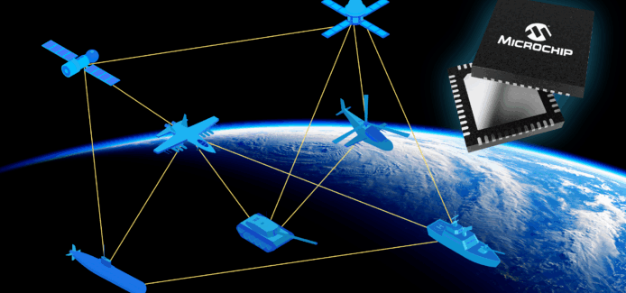
世界的な高周波用窒化ガリウム(RF GaN)市場は、通信インフラの近代化、防衛システムのアップグレード、衛星通信ネットワークの普及が相まって、堅調な拡大を遂げている。 広帯域ギャップ半導体技術であるGaNは、ガリウムヒ素(GaAs)やシリコンベースのLDMOSといった従来材料と比較して優れた性能特性を発揮し、次世代RFアプリケーションに不可欠な高電力密度、高効率、強化された熱管理能力を実現します。
RF GaNデバイス市場は、ニッチな防衛技術から、複数分野にわたる重要インフラを支える主流技術へと進化を遂げている。 市場評価は大幅な成長軌道を示しており、予測期間を通じて業界は15~20%を超える年平均成長率(CAGR)で拡大すると見込まれている。この拡大は、5Gネットワークを展開する通信事業者、レーダーや電子戦能力を近代化する国防省、高性能地上端末や宇宙対応部品を必要とする次世代コンステレーションシステムを打ち上げる衛星事業者からの需要増加を反映している。
通信インフラは最大の応用分野であり、RF GaNデバイス総収益の約40%を占める。世界的な5Gネットワーク展開の継続により、マクロ基地局向け高出力増幅器、大規模MIMOアンテナシステム、スモールセル展開における需要が引き続き牽引されている。 GaN-on-SiC技術は優れた熱伝導性と実証済みの信頼性からこの分野を支配しているが、コスト重視の用途、特に電力要件が控えめなスモールセル展開ではGaN-on-Siが台頭しつつある。将来的には、6G研究プログラムの出現とFR3周波数帯の展開が予想され、ミリ波周波数で動作可能なGaNソリューションへの追加需要が見込まれる。
防衛・航空宇宙アプリケーションは第二の主要市場セグメントであり、軍事レーダーシステム、電子戦装置、安全通信が持続的な需要成長を牽引している。米国防総省はGaNを製造準備レベル10に格上げし、重要防衛プログラム向け量産段階の成熟を表明した。 アクティブ電子走査アレイ(AESA)レーダーシステムはGaNベースの送受信モジュールへの依存度を高めており、電子妨害システムは効果的な妨害・信号妨害のために同技術の広帯域性と高出力能力を活用している。NATO諸国やアジア太平洋諸国における防衛費の増加が、次世代軍事プラットフォームにおけるGaN採用を加速させている。
衛星通信は、低軌道(LEO)コンステレーションシステムと高スループット衛星ゲートウェイの展開に後押しされ、最も急成長している応用分野である。GaNデバイスは地上設置型超小型衛星通信端末(VSAT)においてGaAsソリューションに取って代わりつつあり、耐放射線性バリアントの成熟に伴い宇宙環境対応アプリケーションでの採用も拡大している。
競争環境は依然として集中しており、Wolfspeed、Qorvo、MACOM、住友電気工業、Ampleonなどの主要企業が大きな市場シェアを占めている。 サプライチェーン構造は、集積デバイスメーカー、純粋受託製造ファウンドリ、ファブレス設計会社で構成され、専門的なエピウェハー供給業者や基板メーカーが支援している。特筆すべきは、輸出規制への対応として中国がRF GaNバリューチェーンの急速な現地化を進めており、SICC、Dynax、Sanan ICなどの国内企業が能力を拡大している点である。
技術進化は多方面で継続しており、業界はGaN-on-SiCの4インチから6インチウェーハ生産へ移行中である一方、GaN-on-Si開発は既存技術とのコストパリティ達成に向け200mm、将来的には300mmウェーハフォーマットを目標としている。ダイヤモンドヒートスプレッダーやヘテロジニアス集積技術を採用した先進パッケージングソリューションは、熱管理課題を解決し、高電力密度と要求の厳しいアプリケーション向け信頼性向上を実現している。
世界的な高周波用窒化ガリウム(RF GaN)市場は半導体革新の最前線に立ち、通信、防衛、衛星通信、新興高周波アプリケーションにおける重要な進歩を可能にしている。本包括的市場調査レポートは、2026年から2036年までの重要な10年間にわたるRF GaNエコシステムの詳細な分析を提供し、技術進化、競争力学、サプライチェーン動向、地域別市場機会に関する戦略的洞察を業界関係者に提供する。
RF GaN技術は、ガリウムヒ素(GaAs)やシリコンLDMOSといった従来技術では要求性能レベルを達成できない高電力・高周波アプリケーションにおいて、最適なワイドバンドギャップ半導体ソリューションとしての地位を確固たるものにしています。 この材料の卓越した電子移動度、優れた熱伝導性、高い絶縁破壊電圧により、電力増幅器、モノリシックマイクロ波集積回路(MMIC)、フロントエンドモジュールは、効率性、帯域幅、電力密度指標において既存技術を凌駕します。これらの優位性が、通信インフラ、軍事レーダーシステム、電子戦プラットフォーム、衛星地上端末における採用加速を牽引しています。
通信分野は依然として主要な需要牽引役であり、5Gネットワーク展開ではマクロ基地局、大規模MIMOアンテナシステム、スモールセルアーキテクチャ向けに高効率パワーアンプが求められている。GaN-on-SiC技術は優れた熱管理能力によりプレミアムインフラ分野での優位性を維持する一方、GaN-on-Siは量産用途向けのコスト競争力ある代替技術として台頭している。 2030年代を見据えると、FR3周波数帯で動作する6Gネットワークの展開が予想され、ミリ波動作が可能なRF GaNデバイスに大幅な成長機会をもたらす。
防衛・航空宇宙分野は第二の主要市場基盤であり、世界的な軍事近代化プログラムが能動電子走査アレイ(AESA)レーダーシステム、電子戦ジャマー、安全通信機器、ミサイル防衛システムへの需要を牽引している。過酷な環境下での実証済み信頼性と性能により、主要防衛機関から製造準備認証を取得し、NATO加盟国および同盟国における複数年にわたる生産契約を獲得している。
衛星通信は最も急速に拡大する応用分野であり、低軌道(LEO)コンステレーション展開と高スループット衛星ゲートウェイインフラへの前例のない投資が推進力となっている。GaNデバイスは地上端末におけるGaAsソリューションの代替が進む一方、耐放射線性と長寿命が要求される宇宙応用分野での認定も獲得しつつある。
競争環境では、確立された半導体大手企業群に加え、新興専門企業や、輸出規制への対応として積極的な現地化を進める中国国内産業の台頭が見られる。サプライチェーン分析では、炭化ケイ素基板の供給状況、ガリウム原料の調達、特殊エピタキシャルウェーハ製造能力への依存度が業界構造と地域競争力を左右する重要課題として浮上している。
主要レポート内容
本レポートでは、MACOM Technology Solutions、住友電気デバイスイノベーションズ(SEDI)、Qorvo Inc.、Wolfspeed Inc.、NXP Semiconductors、インフィニオン・テクノロジーズ、STマイクロエレクトロニクス、アナログ・デバイセズ社、Ampleon、三菱電機、富士通、 東芝、RFHIC Corporation、Win Semiconductors、UMS (United Monolithic Semiconductors)、Raytheon Technologies、Northrop Grumman、Lockheed Martin、BAE Systems、Leonardo、Thales Group、Integra Technologies、Custom MMIC、Empower RF Systems、Mission Microwave、Altum RF、 Filtronic、Microchip Technology、Tagore Technology (TagoreTech)、Finwave Semiconductor、Coherent Inc. (II-VI) など... 目次
1 エグゼクティブサマリー
1.1 レポート概要と主な調査結果
1.2 主な市場推進要因と抑制要因
1.3 地域別市場概要
1.4 競争環境の概要
2 市場背景とマクロ経済要因
2.1 世界の半導体業界の概要
2.2 ワイドバンドギャップ半導体材料の展望
2.3 RF デバイス市場の進化
2.4 RF GaN 業界に影響を与える地政学的要因
2.4.1 米中貿易関係と技術制裁
2.4.2 輸出管理規制
2.4.3 戦略的材料への依存 (ガリウム供給)
2.5 規制および政策環境
2.6 世界経済動向の影響
3 市場予測 2026-2036年
3.1 世界の RF GaN デバイス市場予測
3.1.1 年別収益予測 (2026-2036年)
3.1.2 出荷数量予測 (Munits)
3.1.3 期間別CAGR分析
3.2 最終用途別市場予測
3.2.1 通信インフラ
3.2.2 防衛・航空宇宙
3.2.3 衛星通信(SatCom)
3.2.4 消費者/モバイル端末
3.2.5 商用レーダー・航空電子機器
3.2. (ISM アプリケーション)
3.2.7 自動車用レーダー
3.2.8 有線ブロードバンド
3.3 技術プラットフォーム別市場予測
3.3.1 GaN-on-SiC
3.3.2 GaN-on-Si
3.3.3 GaN-on-Diamond (新興)
3.3.4 GaN-on-AlN (新興)
3.3.5 その他の基板
3.4 デバイスカテゴリー別市場予測
3.4.1 ディスクリートRFパワートランジスタ
3.4.2 MMIC(モノリシックマイクロ波集積回路)
3.4.3 パワーアンプ
3.4.4 フロントエンドモジュール
3.4.5 HEMT(高電子移動度トランジスタ)
3.4.6 RF スイッチ
3.4.7 低雑音増幅器 (LNA)
3.5 周波数帯域別市場予測
3.5.1 VHF/UHF (<1 GHz)
3.5.2 L/S バンド (1-4 GHz)
3.5.3 C/X バンド (4-12 GHz)
3.5.4 Ku/Ka-Band (12-40 GHz)
3.5.5 mmWave (>40 GHz)
3.6 GaN RF ウェーハおよびエピウェーハ市場予測
3.6.1 6 インチ相当エピウェーハの収益および数量
3.6.2 ウェーハサイズの内訳 (4 インチ、6 インチ、8 インチ以上)
3.6.3 オープン市場とキャプティブ市場の分析
4 市場の推進要因、抑制要因、および機会
4.1 市場の推進要因
4.1.1 5G/6G ネットワークの展開とインフラのアップグレード
4.1.2 防衛近代化プログラムと軍事費の増加
4.1.3 衛星通信の拡大 (LEOコンステレーション)
4.1.4 GaN技術の優れた性能特性
4.1.5 フェーズドアレイレーダーシステム普及
4.1.6 電子戦近代化
4.2 市場抑制要因
4.2.1 高い製造コスト
4.2.2 基板材料供給制約
4.2.3 ウェーハサイズ移行における技術的課題
4.2.4 GaAs および LDMOS 技術との競争
4.2.5 防衛用途における長い認定サイクル
4.3 市場機会
4.3.1 6G FR3 帯域の展開
4.3.2 自動車用レーダー(79 GHz ADAS/自動運転車)
4.3.3 宇宙および深宇宙用途
4.3.4 RF エネルギー用途(産業用/医療用)
4.3.5 GaN-on-Si コスト削減ロードマップ
4.3.6 先進パッケージング技術
4.4 市場の課題
4.4.1 地政学的緊張とサプライチェーンリスク
4.4.2 信頼性と熱管理
4.4.3 人材と労働力制約
5 アプリケーション市場分析
5.1 テレコムインフラストラクチャ
5.1.1 市場概要と規模
5.1.2 4G/5G 基地局の展開
5.1.3 マッシブ MIMO および能動アンテナシステム
5.1.4 スモールセルおよび無線リモートヘッド (RRH)
5.1.5 バックホールアプリケーション
5.1.6 技術動向 (GaN-on-SiC 対 GaN-on-Si)
5.1.7 6Gのロードマップと影響
5.1.8 主要企業と市場動向
5.2 防衛・航空宇宙
5.2.1 市場概要と規模
5.2.2 軍事レーダーシステム(AESA)
5.2.3 電子戦(妨害装置、対策)
5.2.4 軍事通信
5.2.5 ミサイル防衛および指向性エネルギーシステム
5.2.6 航空機、艦艇、地上プラットフォーム
5.2.7 信頼性の高いファウンドリおよびサプライチェーンの要件
5.2.8 地域防衛支出分析
5.3 衛星通信 (SatCom)
5.3.1 市場の概要と規模
5.3.2 地上システム (VSAT、ゲートウェイ)
5.3.3 宇宙システム (LEO、MEO、 GEO衛星)
5.3.4 高スループット衛星(HTS)
5.3.5 LEOコンステレーション展開(Starlink、OneWeb、Kuiper)
5.3.6 衛星通信におけるGaN対GaAs競争
5.4 消費者向けおよびモバイル端末
5.4.1 市場概要
5.4.2 Sub-6 GHzパワーアンプ (GaAs Dominance)
5.4.3 GaN-on-Si Opportunity in FR3/High-Frequency Bands
5.4.4 WiFi 7 and Future Standards
5.4.5 Wearables and IoT Devices
5.4.6 Barriers to GaN Adoption in Handsets
5.5 Commercial Radar and Avionics
5.5.1 Market Overview and Size
5.5.2 航空管制レーダー
5.5.3 気象レーダーシステム
5.5.4 商用航空電子機器
5.5.5 艦載レーダーアプリケーション
5.6 RFエネルギーおよびISMアプリケーション
5.6.1 市場概要
5.6.2 産業用加熱アプリケーション
5.6.3 医療アプリケーション(MRI、治療用)
5.6.4 プラズマ照明
5.6.5 科学・研究機器
5.7 自動車用レーダー
5.7.1 市場概要と規模
5.7.2 ADASおよび自動運転車アプリケーション
5.7.3 77-79 GHzイメージングレーダー
5.7.4 V2X通信
5.7.5 自動車分野における GaN 採用ロードマップ
6 技術分析
6.1 RF GaN 技術の概要
6.1.1 GaN 材料の特性と利点
6.1.2 競合技術(GaAs、LDMOS、Si)との比較
6.1.3 電力密度と効率指標
6.2 GaN-on-SiC 技術
6.2.1 技術概要と利点
6.2.2 熱伝導率の利点
6.2.3 開発の現状
6.2.4 ウェーハサイズの移行(4インチから6インチ、8インチへ)
6.2.5 製造プロセスと課題
6.2.6 コスト構造分析
6.3 GaN-on-Si 技術
6.3.1 技術概要と価値提案
6.3.2 コスト優位性とスケーラビリティ(200mm、300mm ウェーハ)
6.3.3 技術的課題(熱、RF 性能)
6.3.4 CMOS 互換性と統合
6.3.5 現在の商業状況
6.3.6 コスト競争力へのロードマップ
6.4 新興基板技術
6.4.1 GaN-on-Diamond
6.4.2 GaN-on-AlN
6.4.3 GaN-on-GaN
6.4.4 技術準備レベルと商業化スケジュール
6.5 デバイスアーキテクチャと設計トレンド
6.5.1 HEMTデバイスの進化
6.5.2 ゲート長スケーリング
6.5.3 エンハンスメントモード対デプレッションモードデバイス
6.5.4 マルチステージ増幅器設計
6.6 パッケージング技術
6.6.1 従来型パッケージングソリューション
6.6.2 先進的な熱管理(ダイヤモンドヒートスプレッダー)
6.6.3 フリップチップおよびファンアウトウェーハレベルパッケージング
6.6.4 3D 統合およびヘテロジニアスパッケージング
6.6.5 システムインパッケージ (SiP) ソリューション
6.7 プロセス技術の動向
6.7.1 エピタキシャル成長技術 (MOCVD、MBE)
6.7.2 ゲートプロセスの革新
6.7.3 信頼性および認定基準
7 地域別市場分析
7.1 北米
7.1.1 市場規模および予測
7.1.2 米国市場の動向
7.1.3 防衛・航空宇宙分野における優位性
7.1.4 5Gインフラ投資
7.1.5 CHIPS法と国内製造イニシアチブ
7.1.6 主要プレイヤーと競争環境
7.2 アジア太平洋地域
7.2.1 市場規模と予測
7.2.2 中国市場分析(国内サプライチェーン開発)
7.2.3 日本と韓国
7.2.4 台湾 (先進半導体エコシステム)
7.2.5 東南アジアにおける5G展開
7.2.6 インド防衛・通信市場
7.3 ヨーロッパ
7.3.1 市場規模と予測
7.4 中東・アフリカ
8 サプライチェーン分析
8.1 RF GaNバリューチェーン概要
8.1.1 段階別価値分配
8.2 基板およびウェーハ供給
8.2.1 SiC基板サプライヤー
8.2.2 シリコン基板エコシステム
8.2.3 基板の生産能力と制約
8.2.4 原材料(ガリウム)供給の動向
8.3 エピウェーハ製造
8.3.1 エピウェーハサプライヤー(オープンマーケット)
8.3.2 自社エピタキシー(キャプティブ)
8.3.3 地域別エピウェーハ状況
8.4 デバイス製造
8.4.1 IDMモデル
8.4.2 ファウンドリモデル
8.4.3 ファブレスモデル
8.4.4 ファウンドリ生産能力分析
8.5 パッケージングおよびテスト
8.5.1 2 先進パッケージング技術
8.5.3 試験要件
8.6 システム統合
8.6.1 モジュールメーカー
8.6.2 OEM および Tier 1 インテグレーター
8.7 中国サプライチェーン分析
8.7.1 国内基板およびエピウェハー技術
8.7.2 中国の RF GaN デバイスメーカー
8.7.3 政府支援および政策
7.4 ローカライゼーションの進捗と課題
8.8 サプライチェーンのリスクとレジリエンス
8.8.1 単一障害点
8.8.2 地政学的リスク評価
8.8.3 サプライチェーンの多様化戦略
9 市場見通し
9.1 2026-2036年の市場見通し
9.1.1 短期見通し(2026-2028年)
9.1.2 中期見通し(2029-2032年)
9.1.3 長期見通し(2033-2036年)
9.2 シナリオ分析
9.2.1 ベースケースシナリオ
9.2.2 楽観シナリオ
9.2.3 悲観シナリオ
9.3 技術的混乱シナリオ
9.3.1 GaN-on-Siのブレークスルー
9.4 新興トレンドと将来の発展
9.4.1 RFシステムにおけるAI/ML統合
9.4.2 認知電子戦
9.4.3 サブTHzおよび6Gアプリケーション
9.4.4 宇宙ベースのアプリケーション拡大
10 企業プロファイル (15 社)
10.2 防衛・航空宇宙スペシャリスト (6 社)
10.3 専門および新興企業 (9 社)
10.4 基板およびエピウェハーサプライヤー (7 社)
10.5 中国市場企業 (7社)
10.6 システムインテグレーターおよびOEM (6社)
11 付録
11.1 レポートの目的
11.2 方法論および定義
11.3 略語および略称(拡張)
12 参考文献
図表リスト
表一覧
表1 2026-2036年セグメント別グローバルRF GaN市場概要(収益:百万ドル、数量:万台)
表2 2024-2036年 グローバル半導体市場規模(カテゴリー別)
表3 ガリウム生産量と価格動向
表4 用途別グローバルRF GaNデバイス収益予測、2026-2036年(百万ドル)
表5 用途別世界RF GaNデバイス出荷量予測、2026-2036年 (百万ユニット)
表6 技術プラットフォーム別RF GaN収益、2026-2036年(百万ドル)
表7 RF GaN Revenue by Device Category, 2026-2036 ($M)
表8 RF GaN 収益(周波数帯別)、2026-2036年(百万ドル)
表9 GaN RFエピウェハー売上高(ウェハーサイズ別)、2026-2036年(百万ドル)
表10 GaN RFエピウェハー生産量(ウェハーサイズ別)、2026-2036年(6インチ換算単位)
表11 バックホール用途
表12 技術動向(GaN-on-SiC 対 GaN-on-Si)
表13 テレコムインフラ向けRF GaN市場予測、2026-2036年
表14 防衛・航空宇宙向けRF GaN市場予測、2026-2036年
表15 衛星通信用RF GaN市場予測、2026-2036年
表16 自動車用レーダーRF GaN市場予測、2026-2036年
表17 商用レーダー用RF GaN市場予測、2026-2036年
表18 RFエネルギー用GaN市場予測、2026-2036年
表19 用途別 周波数と電力要件
表20 5Gから6Gへの進化タイムラインとRF GaNの意義
表21 プラットフォーム別防衛アプリケーションのセグメンテーション
表22 技術プラットフォーム比較マトリックス
表23 ノード別GaNプロセス技術ロードマップ
表24 パッケージング技術比較
表25 GaN vs GaAs vs LDMOS vs Si 性能比較
表26 GaN-on-SiC vs GaN-on-Si 技術のトレードオフ
表27 基板別熱伝導率比較
表28 デバイスゲート長スケーリングの傾向
表29 地域別RF GaN市場予測、2026-2036年(百万ドル)
表30 国別市場規模推定値
表31 地域別市場シェア比較、2026年対2036年
表32 GaN RFサプライチェーン企業マッピング
表33 SiC基板サプライヤーの生産能力分析
表34 GaN RFファウンドリ生産能力(ウェーハサイズ別)
表35 中国RF GaNサプライチェーン主要企業
表36 サプライチェーンビジネスモデル比較(IDM vs ファウンドリ vs ファブレス)
表37 SiCウェハー需給バランス予測
図一覧
図1 世界のRF GaN市場規模と成長軌跡、2026-2036年
図2 用途別市場シェア(2026年 vs 2031年 vs 2036年)
図3 ワイドバンドギャップ半導体材料比較(GaN vs SiC vs GaAs vs Si)
図4 世界のRFデバイス産業市場規模予測、2024-2036年
図5 RF GaNデバイス市場収益予測、2026-2036年
図6 用途別市場シェア、2026-2031-2036年比較
図7 GaN-on-SiC対GaN-on-Si市場シェア推移
図8 デバイスカテゴリー別市場シェア内訳
図9 周波数帯別収益分布
図10 エピウェハー市場規模予測(オープン vs キャプティブ)
図11 市場推進要因と抑制要因の影響分析
図12 RF GaN市場におけるポーターの5つの力分析
図13 RF GaN産業のSWOT分析
図14 6Gロードマップとその影響
図15 自動車用レーダー技術ロードマップ
図16 ウェーハサイズ進化のタイムライン
図17 先進パッケージング技術の進化
図18 中国におけるRF GaNの現地化進捗タイムライン

Summary
The global Radio Frequency Gallium Nitride (RF GaN) market is experiencing robust expansion, driven by the convergence of telecommunications infrastructure modernization, defense system upgrades, and the proliferation of satellite communication networks. As a wide-bandgap semiconductor technology, GaN delivers superior performance characteristics compared to legacy materials such as gallium arsenide (GaAs) and silicon-based LDMOS, enabling higher power density, greater efficiency, and enhanced thermal management capabilities that are essential for next-generation RF applications.
The RF GaN device market has evolved from a niche defense-focused technology to a mainstream enabler of critical infrastructure across multiple sectors. Market valuations indicate substantial growth trajectories, with the industry projected to expand at compound annual growth rates exceeding 15-20% through the forecast period. This expansion reflects increasing demand from telecommunications operators deploying 5G networks, defense ministries modernizing radar and electronic warfare capabilities, and satellite operators launching next-generation constellation systems requiring high-performance ground terminals and space-qualified components.
Telecommunications infrastructure represents the largest application segment, commanding approximately 40% of total RF GaN device revenues. The ongoing global rollout of 5G networks continues driving demand for high-power amplifiers in macro base stations, massive MIMO antenna systems, and small cell deployments. GaN-on-SiC technology dominates this segment due to its superior thermal conductivity and proven reliability, though GaN-on-Si is gaining traction for cost-sensitive applications, particularly in small cell deployments where power requirements are more modest. Looking ahead, the emergence of 6G research programs and the anticipated FR3 frequency band deployments are expected to create additional demand for GaN solutions capable of operating at millimeter-wave frequencies.
Defense and aerospace applications constitute the second major market segment, with military radar systems, electronic warfare equipment, and secure communications driving consistent demand growth. The U.S. Department of Defense has elevated GaN to Manufacturing Readiness Level 10, signaling full production maturity for critical defense programs. Active electronically scanned array (AESA) radar systems increasingly rely on GaN-based transmit/receive modules, while electronic countermeasure systems leverage the technology's wide bandwidth and high power capabilities for effective jamming and signal disruption. Defense spending increases across NATO countries and Asia-Pacific nations are accelerating GaN adoption in next-generation military platforms.
Satellite communications represent the fastest-growing application segment, propelled by the deployment of low-earth orbit (LEO) constellation systems and high-throughput satellite gateways. GaN devices are displacing GaAs solutions in ground-based very small aperture terminals (VSATs) and gaining adoption in space-qualified applications as radiation-hardened variants mature.
The competitive landscape remains concentrated, with leading players including Wolfspeed, Qorvo, MACOM, Sumitomo Electric, and Ampleon commanding significant market share. The supply chain structure encompasses integrated device manufacturers, pure-play foundries, and fabless design houses, supported by specialized epiwafer suppliers and substrate manufacturers. Notably, China is rapidly localizing its RF GaN value chain in response to export restrictions, with domestic players such as SICC, Dynax, and Sanan IC expanding capabilities.
Technology evolution continues across multiple fronts, with the industry transitioning from 4-inch to 6-inch wafer production for GaN-on-SiC, while GaN-on-Si development targets 200mm and potentially 300mm wafer formats to achieve cost parity with incumbent technologies. Advanced packaging solutions incorporating diamond heat spreaders and heterogeneous integration approaches are addressing thermal management challenges, enabling higher power densities and improved reliability for demanding applications.
The global Radio Frequency Gallium Nitride (RF GaN) market stands at the forefront of semiconductor innovation, enabling critical advances across telecommunications, defense, satellite communications, and emerging high-frequency applications. This comprehensive market intelligence report delivers in-depth analysis of the RF GaN ecosystem spanning the pivotal decade from 2026 to 2036, equipping industry stakeholders with strategic insights into technology evolution, competitive dynamics, supply chain developments, and regional market opportunities.
RF GaN technology has firmly established itself as the preferred wide-bandgap semiconductor solution for high-power, high-frequency applications where legacy technologies such as gallium arsenide (GaAs) and silicon LDMOS cannot deliver required performance levels. The material's exceptional electron mobility, superior thermal conductivity, and high breakdown voltage enable power amplifiers, monolithic microwave integrated circuits (MMICs), and front-end modules that outperform incumbent technologies across efficiency, bandwidth, and power density metrics. These advantages are driving accelerating adoption across telecommunications infrastructure, military radar systems, electronic warfare platforms, and satellite ground terminals.
The telecommunications sector remains the dominant demand driver, with 5G network deployments requiring high-efficiency power amplifiers for macro base stations, massive MIMO antenna systems, and small cell architectures. GaN-on-SiC technology continues commanding the premium infrastructure segment due to superior thermal management capabilities, while GaN-on-Si emerges as a cost-competitive alternative for volume applications. Looking toward the 2030s, the anticipated deployment of 6G networks operating in FR3 frequency bands presents substantial growth opportunities for RF GaN devices capable of millimeter-wave operation.
Defence and aerospace applications constitute the second major market pillar, with military modernization programs worldwide driving demand for active electronically scanned array (AESA) radar systems, electronic warfare jammers, secure communications equipment, and missile defense systems. The technology's proven reliability and performance under extreme conditions has earned manufacturing readiness certification from major defense agencies, unlocking multi-year production contracts across NATO countries and allied nations.
Satellite communications represent the fastest-expanding application segment, propelled by unprecedented investment in low-earth orbit (LEO) constellation deployments and high-throughput satellite gateway infrastructure. GaN devices increasingly displace GaAs solutions in ground-based terminals while gaining qualification for space-based applications requiring radiation tolerance and long operational lifetimes.
The competitive landscape features a concentrated group of established semiconductor leaders alongside emerging specialists and an increasingly capable Chinese domestic industry responding to export restrictions through aggressive localization efforts. Supply chain analysis reveals critical dependencies on silicon carbide substrate availability, gallium raw material supply, and specialized epitaxial wafer manufacturing capacity that shape industry structure and regional competitive positioning.
Key Report Contents include
This report features comprehensive profiles of 43 companies across the RF GaN value chain including MACOM Technology Solutions, Sumitomo Electric Device Innovations (SEDI), Qorvo Inc., Wolfspeed Inc., NXP Semiconductors, Infineon Technologies, STMicroelectronics, Analog Devices Inc., Ampleon, Mitsubishi Electric, Fujitsu, Toshiba, RFHIC Corporation, Win Semiconductors, UMS (United Monolithic Semiconductors), Raytheon Technologies, Northrop Grumman, Lockheed Martin, BAE Systems, Leonardo, Thales Group, Integra Technologies, Custom MMIC, Empower RF Systems, Mission Microwave, Altum RF, Filtronic, Microchip Technology, Tagore Technology (TagoreTech), Finwave Semiconductor, Coherent Inc. (II-VI) and more.... Table of Contents
1 EXECUTIVE SUMMARY
1.1 Report Overview and Key Findings
1.2 Key Market Drivers and Restraints
1.3 Regional Market Summary
1.4 Competitive Landscape Overview
2 MARKET CONTEXT AND MACROECONOMIC FACTORS
2.1 Global Semiconductor Industry Overview
2.2 Wide-Bandgap Semiconductor Materials Landscape
2.3 RF Device Market Evolution
2.4 Geopolitical Factors Affecting the RF GaN Industry
2.4.1 US-China Trade Relations and Technology Sanctions
2.4.2 Export Control Regulations
2.4.3 Strategic Material Dependencies (Gallium Supply)
2.5 Regulatory and Policy Environment
2.6 Impact of Global Economic Trends
3 MARKET FORECASTS 2026-2036
3.1 Global RF GaN Device Market Forecast
3.1.1 Revenue Forecast by Year (2026-2036)
3.1.2 Shipment Volume Forecast (Munits)
3.1.3 CAGR Analysis by Period
3.2 Market Forecast by End-Use Application
3.2.1 Telecom Infrastructure
3.2.2 Defense and Aerospace
3.2.3 Satellite Communications (SatCom)
3.2.4 Consumer/Mobile Handsets
3.2.5 Commercial Radar and Avionics
3.2.6 RF Energy (ISM Applications)
3.2.7 Automotive Radar
3.2.8 Wired Broadband
3.3 Market Forecast by Technology Platform
3.3.1 GaN-on-SiC
3.3.2 GaN-on-Si
3.3.3 GaN-on-Diamond (Emerging)
3.3.4 GaN-on-AlN (Emerging)
3.3.5 Other Substrates
3.4 Market Forecast by Device Category
3.4.1 Discrete RF Power Transistors
3.4.2 MMICs (Monolithic Microwave Integrated Circuits)
3.4.3 Power Amplifiers
3.4.4 Front-End Modules
3.4.5 HEMTs (High Electron Mobility Transistors)
3.4.6 RF Switches
3.4.7 Low Noise Amplifiers (LNAs)
3.5 Market Forecast by Frequency Band
3.5.1 VHF/UHF (<1 GHz)
3.5.2 L/S-Band (1-4 GHz)
3.5.3 C/X-Band (4-12 GHz)
3.5.4 Ku/Ka-Band (12-40 GHz)
3.5.5 mmWave (>40 GHz)
3.6 GaN RF Wafer and Epiwafer Market Forecast
3.6.1 6-Inch Equivalent Epiwafer Revenue and Volume
3.6.2 Wafer Size Breakdown (4", 6", 8"+)
3.6.3 Open Market vs Captive Market Analysis
4 MARKET DRIVERS, RESTRAINTS, AND OPPORTUNITIES
4.1 Market Drivers
4.1.1 5G/6G Network Deployment and Infrastructure Upgrades
4.1.2 Defence Modernization Programs and Increased Military Spending
4.1.3 Satellite Communication Expansion (LEO Constellations)
4.1.4 Superior Performance Characteristics of GaN Technology
4.1.5 Phased Array Radar System Proliferation
4.1.6 Electronic Warfare Modernization
4.2 Market Restraints
4.2.1 High Manufacturing Costs
4.2.2 Substrate Material Supply Constraints
4.2.3 Technical Challenges in Wafer Size Transition
4.2.4 Competition from GaAs and LDMOS Technologies
4.2.5 Long Qualification Cycles for Defense Applications
4.3 Market Opportunities
4.3.1 6G FR3 Band Deployment
4.3.2 Automotive Radar (79 GHz ADAS/Autonomous Vehicles)
4.3.3 Space and Deep-Space Applications
4.3.4 RF Energy Applications (Industrial/Medical)
4.3.5 GaN-on-Si Cost Reduction Roadmap
4.3.6 Advanced Packaging Technologies
4.4 Market Challenges
4.4.1 Geopolitical Tensions and Supply Chain Risks
4.4.2 Reliability and Thermal Management
4.4.3 Talent and Workforce Constraints
5 APPLICATION MARKET ANALYSIS
5.1 Telecom Infrastructure
5.1.1 Market Overview and Size
5.1.2 4G/5G Base Station Deployments
5.1.3 Massive MIMO and Active Antenna Systems
5.1.4 Small Cells and Radio Remote Heads (RRH)
5.1.5 Backhaul Applications
5.1.6 Technology Trends (GaN-on-SiC vs GaN-on-Si)
5.1.7 6G Roadmap and Implications
5.1.8 Key Players and Market Dynamics
5.2 Defence and Aerospace
5.2.1 Market Overview and Size
5.2.2 Military Radar Systems (AESA)
5.2.3 Electronic Warfare (Jammers, Countermeasures)
5.2.4 Military Communications
5.2.5 Missile Defence and Directed Energy Systems
5.2.6 Airborne, Naval, and Ground-Based Platforms
5.2.7 Trusted Foundry and Supply Chain Requirements
5.2.8 Regional Defence Spending Analysis
5.3 Satellite Communications (SatCom)
5.3.1 Market Overview and Size
5.3.2 Ground-Based Systems (VSAT, Gateways)
5.3.3 Space-Based Systems (LEO, MEO, GEO Satellites)
5.3.4 High-Throughput Satellites (HTS)
5.3.5 LEO Constellation Deployments (Starlink, OneWeb, Kuiper)
5.3.6 GaN vs GaAs Competition in SatCom
5.4 Consumer and Mobile Handsets
5.4.1 Market Overview
5.4.2 Sub-6 GHz Power Amplifiers (GaAs Dominance)
5.4.3 GaN-on-Si Opportunity in FR3/High-Frequency Bands
5.4.4 WiFi 7 and Future Standards
5.4.5 Wearables and IoT Devices
5.4.6 Barriers to GaN Adoption in Handsets
5.5 Commercial Radar and Avionics
5.5.1 Market Overview and Size
5.5.2 Air Traffic Control Radar
5.5.3 Weather Radar Systems
5.5.4 Commercial Avionics
5.5.5 Shipborne Radar Applications
5.6 RF Energy and ISM Applications
5.6.1 Market Overview
5.6.2 Industrial Heating Applications
5.6.3 Medical Applications (MRI, Therapeutic)
5.6.4 Plasma Lighting
5.6.5 Scientific and Research Equipment
5.7 Automotive Radar
5.7.1 Market Overview and Size
5.7.2 ADAS and Autonomous Vehicle Applications
5.7.3 77-79 GHz Imaging Radar
5.7.4 V2X Communications
5.7.5 GaN Adoption Roadmap in Automotive
6 TECHNOLOGY ANALYSIS
6.1 RF GaN Technology Overview
6.1.1 GaN Material Properties and Advantages
6.1.2 Comparison with Competing Technologies (GaAs, LDMOS, Si)
6.1.3 Power Density and Efficiency Metrics
6.2 GaN-on-SiC Technology
6.2.1 Technology Overview and Advantages
6.2.2 Thermal Conductivity Benefits
6.2.3 Current State of Development
6.2.4 Wafer Size Transition (4" to 6" to 8")
6.2.5 Manufacturing Process and Challenges
6.2.6 Cost Structure Analysis
6.3 GaN-on-Si Technology
6.3.1 Technology Overview and Value Proposition
6.3.2 Cost Advantages and Scalability (200mm, 300mm Wafers)
6.3.3 Technical Challenges (Thermal, RF Performance)
6.3.4 CMOS Compatibility and Integration
6.3.5 Current Commercial Status
6.3.6 Roadmap to Cost Competitiveness
6.4 Emerging Substrate Technologies
6.4.1 GaN-on-Diamond
6.4.2 GaN-on-AlN
6.4.3 GaN-on-GaN
6.4.4 Technology Readiness Levels and Commercialization Timeline
6.5 Device Architecture and Design Trends
6.5.1 HEMT Device Evolution
6.5.2 Gate Length Scaling
6.5.3 Enhancement-Mode vs Depletion-Mode Devices
6.5.4 Multi-Stage Amplifier Design
6.6 Packaging Technologies
6.6.1 Traditional Packaging Solutions
6.6.2 Advanced Thermal Management (Diamond Heat-Spreaders)
6.6.3 Flip-Chip and Fan-Out Wafer-Level Packaging
6.6.4 3D Integration and Heterogeneous Packaging
6.6.5 System-in-Package (SiP) Solutions
6.7 Process Technology Trends
6.7.1 Epitaxial Growth Techniques (MOCVD, MBE)
6.7.2 Gate Process Innovations
6.7.3 Reliability and Qualification Standards
7 REGIONAL MARKET ANALYSIS
7.1 North America
7.1.1 Market Size and Forecast
7.1.2 United States Market Dynamics
7.1.3 Defense and Aerospace Dominance
7.1.4 5G Infrastructure Investments
7.1.5 CHIPS Act and Domestic Manufacturing Initiatives
7.1.6 Key Players and Competitive Landscape
7.2 Asia-Pacific
7.2.1 Market Size and Forecast
7.2.2 China Market Analysis (Domestic Supply Chain Development)
7.2.3 Japan and South Korea
7.2.4 Taiwan (Advanced Semiconductor Ecosystem)
7.2.5 Southeast Asia 5G Rollout
7.2.6 India Defence and Telecom Market
7.3 Europe
7.3.1 Market Size and Forecast
7.4 Middle East and Africa
8 SUPPLY CHAIN ANALYSIS
8.1 RF GaN Value Chain Overview
8.1.1 End-to-End Supply Chain Map
8.1.2 Value Distribution by Stage
8.2 Substrate and Wafer Supply
8.2.1 SiC Substrate Suppliers
8.2.2 Silicon Substrate Ecosystem
8.2.3 Substrate Capacity and Constraints
8.2.4 Raw Material (Gallium) Supply Dynamics
8.3 Epiwafer Manufacturing
8.3.1 Epiwafer Suppliers (Open Market)
8.3.2 In-House Epitaxy (Captive)
8.3.3 Regional Epiwafer Landscape
8.4 Device Fabrication
8.4.1 IDM Model
8.4.2 Foundry Model
8.4.3 Fabless Model
8.4.4 Foundry Capacity Analysis
8.5 Packaging and Testing
8.5.1 OSAT Providers
8.5.2 Advanced Packaging Capabilities
8.5.3 Testing Requirements
8.6 System Integration
8.6.1 Module Manufacturers
8.6.2 OEM and Tier 1 Integrators
8.7 China Supply Chain Analysis
8.7.1 Domestic Substrate and Epiwafer Capabilities
8.7.2 Chinese RF GaN Device Manufacturers
8.7.3 Government Support and Policy
8.7.4 Localization Progress and Challenges
8.8 Supply Chain Risks and Resilience
8.8.1 Single Points of Failure
8.8.2 Geopolitical Risk Assessment
8.8.3 Supply Chain Diversification Strategies
9 MARKET OUTLOOK
9.1 Market Outlook 2026-2036
9.1.1 Near-Term Outlook (2026-2028)
9.1.2 Medium-Term Outlook (2029-2032)
9.1.3 Long-Term Outlook (2033-2036)
9.2 Scenario Analysis
9.2.1 Base Case Scenario
9.2.2 Optimistic Scenario
9.2.3 Pessimistic Scenario
9.3 Technology Disruption Scenarios
9.3.1 GaN-on-Si Breakthrough
9.4 Emerging Trends and Future Developments
9.4.1 AI/ML Integration in RF Systems
9.4.2 Cognitive Electronic Warfare
9.4.3 Sub-THz and 6G Applications
9.4.4 Space-Based Applications Expansion
10 COMPANY PROFILES
10.1 DEVICE MANUFACTURERS (15 company profiles)
10.2 DEFENCE AND AEROSPACE SPECIALISTS (6 company profiles)
10.3 SPECIALTY AND EMERGING PLAYERS (9 company profiles)
10.4 SUBSTRATE AND EPIWAFER SUPPLIERS (7 company profiles)
10.5 CHINESE MARKET PLAYERS (7 company profiles)
10.6 SYSTEM INTEGRATORS AND OEMs (6 company profiles)
11 APPENDICES
11.1 Report Objectives
11.2 Methodology and Definitions
11.3 Acronyms and Abbreviations (Extended)
12 REFERENCES
List of Tables/Graphs
List of Tables
Table1 Global RF GaN Market Summary by Segment, 2026-2036 (Revenue $M, Volume Munits)
Table2 Global Semiconductor Market Size by Category, 2024-2036
Table3 Gallium Production and Pricing Trends
Table4 Global RF GaN Device Revenue Forecast by Application, 2026-2036 ($M)
Table5 Global RF GaN Device Shipment Forecast by Application, 2026-2036 (Munits)
Table6 RF GaN Revenue by Technology Platform, 2026-2036 ($M)
Table7 RF GaN Revenue by Device Category, 2026-2036 ($M)
Table8 RF GaN Revenue by Frequency Band, 2026-2036 ($M)
Table9 GaN RF Epiwafer Revenue by Wafer Size, 2026-2036 ($M)
Table10 GaN RF Epiwafer Volume by Wafer Size, 2026-2036 (6" Equivalent Units)
Table11 Backhaul Applications
Table12 Technology Trends (GaN-on-SiC vs GaN-on-Si)
Table13 Telecom Infrastructure RF GaN Market Forecast, 2026-2036
Table14 Defense and Aerospace RF GaN Market Forecast, 2026-2036
Table15 SatCom RF GaN Market Forecast, 2026-2036
Table16 Automotive Radar RF GaN Market Forecast, 2026-2036
Table17 Commercial Radar RF GaN Market Forecast, 2026-2036
Table18 RF Energy RF GaN Market Forecast, 2026-2036
Table19 Frequency vs Power Requirements by Application
Table20 5G to 6G Evolution Timeline and RF GaN Implications
Table21 Defence Application Segmentation by Platform
Table22 Technology Platform Comparison Matrix
Table23 GaN Process Technology Roadmap by Node
Table24 Packaging Technology Comparison
Table25 GaN vs GaAs vs LDMOS vs Si Performance Comparison
Table26 GaN-on-SiC vs GaN-on-Si Technology Trade-offs
Table27 Thermal Conductivity Comparison by Substrate
Table28 Device Gate Length Scaling Trend
Table29 Regional RF GaN Market Forecast, 2026-2036 ($M)
Table30 Country-Level Market Size Estimates
Table31 Regional Market Share Comparison, 2026 vs 2036
Table32 GaN RF Supply Chain Player Mapping
Table33 SiC Substrate Supplier Capacity Analysis
Table34 GaN RF Foundry Capacity by Wafer Size
Table35 China RF GaN Supply Chain Players
Table36 Supply Chain Business Model Comparison (IDM vs Foundry vs Fabless)
Table37 SiC Wafer Supply-Demand Balance Forecast
List of Figures
Figure1 Global RF GaN Market Size and Growth Trajectory, 2026-2036
Figure2 Market Share by End-Use Application (2026 vs 2031 vs 2036)
Figure3 Wide-Bandgap Semiconductor Material Comparison (GaN vs SiC vs GaAs vs Si)
Figure4 Global RF Device Industry Market Size Projection, 2024-2036
Figure5 RF GaN Device Market Revenue Forecast, 2026-2036
Figure6 Market Share by Application, 2026-2031-2036 Comparison
Figure7 GaN-on-SiC vs GaN-on-Si Market Share Evolution
Figure8 Device Category Market Share Breakdown
Figure9 Frequency Band Revenue Distribution
Figure10 Epiwafer Market Size Projection (Open vs Captive)
Figure11 Market Drivers and Restraints Impact Analysis
Figure12 Porter's Five Forces Analysis for RF GaN Market
Figure13 SWOT Analysis of RF GaN Industry
Figure14 6G Roadmap and Implications
Figure15 Automotive Radar Technology Roadmap
Figure16 Wafer Size Evolution Timeline
Figure17 Advanced Packaging Technology Evolution
Figure18 China RF GaN Localization Progress Timeline
ご注文は、お電話またはWEBから承ります。お見積もりの作成もお気軽にご相談ください。本レポートと同分野(通信・IT)の最新刊レポート
Future Markets, inc.社の 5G & 6G分野 での最新刊レポートよくあるご質問Future Markets, inc.社はどのような調査会社ですか?Future Markets, inc.は先端技術に焦点をあてたスウェーデンの調査会社です。 2009年設立のFMi社は先端素材、バイオ由来の素材、ナノマテリアルの市場をトラッキングし、企業や学... もっと見る 調査レポートの納品までの日数はどの程度ですか?在庫のあるものは速納となりますが、平均的には 3-4日と見て下さい。
注文の手続きはどのようになっていますか?1)お客様からの御問い合わせをいただきます。
お支払方法の方法はどのようになっていますか?納品と同時にデータリソース社よりお客様へ請求書(必要に応じて納品書も)を発送いたします。
データリソース社はどのような会社ですか?当社は、世界各国の主要調査会社・レポート出版社と提携し、世界各国の市場調査レポートや技術動向レポートなどを日本国内の企業・公官庁及び教育研究機関に提供しております。
|
|

