世界各国のリアルタイムなデータ・インテリジェンスで皆様をお手伝い
世界の半導体製造装置:市場、市場シェア、市場予測Global Semiconductor Equipment: Markets, Market Shares and Market Forecasts 本レポートでは、半導体製造装置市場について24以上の分野別に解説し、米国、欧州、アジアの主要装置メーカー43社を紹介している。各分野における各社の市場シェアを示し、各分野の予測も行っている。 *20... もっと見る
本レポートは毎月更新を行っています。最新情報はお気軽にお問合せください。

サマリー
本レポートでは、半導体製造装置市場について24以上の分野別に解説し、米国、欧州、アジアの主要装置メーカー43社を紹介している。各分野における各社の市場シェアを示し、各分野の予測も行っている。 *2013年から2024年までの24セグメントにおける各競合企業の市場収益のエクセル・スプレッドシート付き。エクセルスプレッドシートは本ウェブサイトからのご注文時のみご利用いただけます。
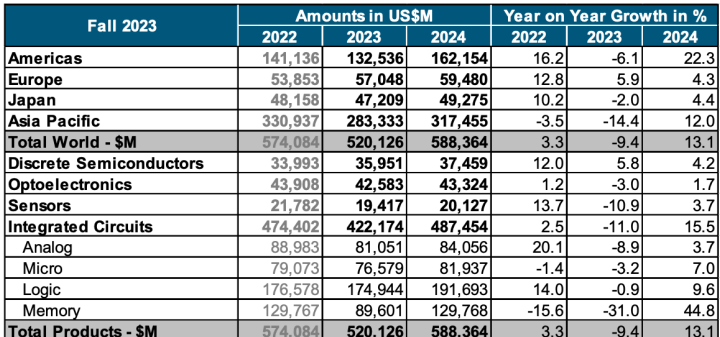
Semiconductor Industry Association(SIA)の発表によると、2023年の世界半導体業界販売高が$5268 billionとなり、業界過去最高の年間合計であった2022年の$5741 billionに比べ8.2%減少している。売上高は2023年後半に回復した。実際、第4四半期の売上高は1,460億ドルで、2022年第4四半期の合計を11.6%上回り、2023年第3四半期の合計を8.4%上回った。また、2023年12月の世界売上高は486億ドルで、2023年11月の合計と比較して1.5%増加した。月次販売高は、World Semiconductor Trade Statistics(WSTS)組織によって集計され、3ヶ月移動平均を表している。SIAは、売上高で米国半導体業界の99%を代表しており、米国以外のチップ企業のほぼ3分の2を代表している。
地域別では、欧州が2023年の年間販売高が4.0%増と唯一成長した地域市場である。2023年の他のすべての地域市場の年間売上高は減少した:日本(-3.1%)、米州(-5.2%)、AsiaPacific/All Other(-10.1%)、中国(-14.0%)である。2023年12月の月次売上高は、中国(4.7%増)、米州(1.8%増)、AsiaPacific/All Other(0.3%増)で2023年11月に比べ増加したが、日本(2.4%減)、欧州(3.9%減)で減少した。
2023年にはいくつかの半導体製品分野が目立った。ロジック製品の2023年の売上高は1,785億ドルとなり、売上高で最大の製品分野となった。メモリー製品の売上高は923億ドルで第2位であった。マイクロコントローラー・ユニット(MCU)は11.4%増の合計279億ドル。また、車載用ICの売上高は前年同期比23.7%増の422億ドルとなり、過去最高を記録した。
世界的な景気減速と岬の過剰支出が、半導体の供給過剰と2023年の設備メルトダウンを生み出すきっかけとなった。現在のfabsが拡大し、新しいfabsが計画される中、大幅なcapacity拡大が進行中である。
米国の自給率を向上させ、アジアへの依存を減らすために国内製造設備に$500 billionを投資するというBiden政権の推進が、供給過剰と生産能力拡大をもたらす可能性の高いコースを開始した:
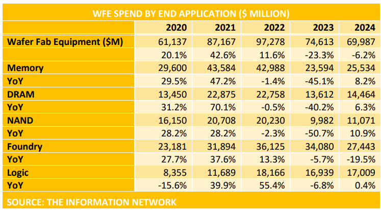
2020年から2024年にかけての最終製品別ウェーハフロントエンド装置投資額を以下に示す
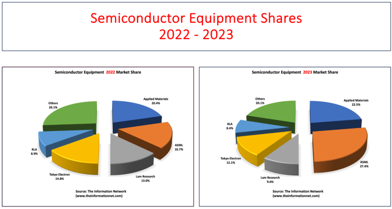
以下の図1.1では、2022年と2023年の世界WFE装置市場の市場シェアを示しており、世界の装置企業トップ5とその他の装置企業のシェアを掲載している。
 業界動向
半導体の使用の増加は、その複雑性の増加を伴っている。半導体の新たな用途や市場の創出により、サプライヤーやメーカーは、より高機能・高性能でありながら低価格を実現する新製品への需要の高まりに直面している。その結果、多くの新しい複雑な材料、構造、プロセスが半導体製造のエコシステムに導入されている。
そのような材料には、銅、低誘電率および高誘電率誘電体、シリコン・オン・インシュレーター、シリコン・ゲルマニウム、III-V、歪みシリコン、ソース/ドレイン引き上げなどがあります。メーカーは過去数年間、(200mmシリコン・ウエハから)300mmシリコン・ウエハへと移行してきました。300mmウェーハは、200mmウェーハの最大2倍の集積回路を生産できる一方で、新たな製造上の課題も生じている。例えば、300mmウェーハは200mmウェーハの2倍以上曲がったり反ったりするため、ダメージを受けやすい。また、300mmウェーハは面積が大きいため、ウェーハ全体の膜の均一性を保つことが難しくなります。
半導体はまた、3D FinFETトランジスタ、GAA(ゲート・オール・アラウンド)、3D-NAND、新興メモリ構造など、より微細で複雑な構造へと移行し続けている。半導体デバイスの複雑化は、半導体製造プロセスの複雑さとコストを増大させ、これが計測システムに対する需要拡大の原動力にもなっている。
ますます複雑化し、フィーチャー・サイズが小さくなっているため、半導体製造装置のコストと性能に対する要求も大幅に増加している。メーカーが利用する自動化レベルが高くなったため、ウエハー製造装置のコストも上昇している。したがって、半導体メーカーは、技術的リーダーシップを維持し、製造能力を拡大し、収益性を維持するために、設備投資を増やさなければならない。
製造工程の多くは、ウェハーへの、またはウェハーからの材料の層の制御された塗布または除去を含む。ウェハーへの材料の塗布は蒸着と呼ばれ、電気絶縁性、導電性または半導電性の材料の極めて薄い膜の積層を伴う。これらの層は、厚さが1000分の1から10万分の1ミリメートル以下のものまであり、ウェハとその表面に電気的に活性な領域を作ります。
ウェハー上に薄膜層を形成し、特定の性能特性を実現するために、さまざまな材料や成膜プロセスが用いられている。薄膜層の主な成膜方法のひとつが化学気相成長法(CVD)である。CVDでは、ウェハーを処理するチャンバー内に化学物質を導入し、熱と化学反応を利用して蒸着させ、シリコンウェーハーの表面に固体材料の層を形成します。
CVD装置が最大の装置タイプであるが、薄膜形成装置市場にはエピタキシー、物理蒸着(PVD)、原子層蒸着(ALD)といったより多くのセグメントがある。現在、ALDは最も急成長している装置カテゴリーである。計測システムは、成膜プロセス中の薄膜層の厚さと均一性をモニターする。
フォトリソグラフィ・プロセスが適切に機能するためには、フォトレジストの厚さが正確で均一でなければなりません。さらに、フォトリソグラフィープロセスを制御するために、膜厚、反射率、オーバーレイレジストレーション、重要寸法がすべて測定され、検証されます。露光されたフォトレジストは、薬液にかけられると現像されます。現像されたウェハは、次に別の化学溶液(プラズマ)にさらされ、フォトレジストで覆われていない部分をエッチングして集積回路の構造を作ります。半導体メーカーは、エッチングプロセスによる材料の除去と、作成された構造の重要な寸法を検証するために、計測システムを使用しています。
半導体製造業界には、より効果的なプロセス制御ソリューションの必要性を高める技術的・業務的なトレンドが数多くあります。これらの傾向には以下が含まれる
・半導体フィーチャーの小型化。より小さく、より効率的なチップを求める動きは続いており、主要メーカーは5nm、3nm、さらには2nmのプロセス・ノードを目指している。
・3D デバイス構造への移行。ファウンドリは3D FinFETトランジスタを採用している。2019年に生産された主要ロジック・プロセスは、インテルの10nmプロセス、サムスンの7nmプロセス、TSMCの7nm光プロセス(7FF)であった。2019年末には、サムスンとTSMCがともに5nmプロセスのリスク生産を開始し、2020年には両プロセスとも生産が開始された。
・メモリーメーカーは、次世代 NAND 技術の 300 層 3D NAND や垂直構造への移行を進めている。これらのトレンドは、現在光学計測技術によってのみサポートされているこれらの3D構造の重要な寸法を測定できる計測ソリューションによるプロセス制御を必要とする。
・3D 統合技術への移行。複数のICチップを直接接続するアクティブ・デバイスの3次元(3D)集積は、電力効率、性能向上、製品の大幅な小型化、コスト削減など、多くの利点をもたらす。3D集積はムーアの法則を拡張する新たな方法を提供する。
TSVは積層チップ間の高帯域幅相互接続を実現します。TSVプロセスは生産段階に入り始めている。TSVの場合、複数のチップが接続されるため、経済的に実行可能なプロセスとするためには、非常に高い歩留まりレベルを達成し、維持する必要がある。TSV の計測ソリューションには、深さ、側壁の傾斜、上下の直径(CD)、底面の曲率を綿密に監視・測定することが要求される。
・パワーエレクトロニクスやRFアプリケーションでは、SiCやGaN材料へのシフトが著しい。これらの材料は、効率、耐熱性、パワーハンドリング、特に高電圧・高周波において優れた性能を発揮する。このため、電気自動車、再生可能エネルギー・システム、5Gネットワークなどの用途に特に適しており、これらの特性により、より効率的でコンパクトな信頼性の高いシステムを実現することができる。
・EUVリソグラフィの利用拡大。リソグラフィ。業界のムーアの法則へのあくなき追求は、先進的なプロセス・ノードの開発を推進し、現在では 3nm に近づきつつあり、2nm 技術も視野に入っている。極端紫外線(EUV)リソグラフィは、この進化において極めて重要な役割を果たしており、
複雑なマルチパターニング技術を必要とすることなく、より微細なフィーチャ・パターニングを
可能にすることで、より小さく複雑な回路の作成を可能にして
います。このリソグラフィ技術の飛躍は、半導体の微細化と性能向上のペースを維持するために不可欠である。
・新材料。2012 年以降、テクノロジー・ノードのフィーチャーが縮小し続け、3D トランジスター(FinFET 設計)が導入されるにつれて、厚さ、フィーチャー・カバレッジ、応力、電気的、機械的要件が厳密な高品質の誘電体膜の成膜に依存する重要なプロセス工程が増えてきた。
・鋳造製造の成長。半導体プロセスの開発と生産に必要な投資が増加し、さまざまな種類の半導体が急増した結果、半導体製造は、大規模な半導体受託製造業者(ファウンドリ)に委託されることが増えている。ファウンドリーは通常、複数の異なるプロセスを実行
し、1つの設備で数百から数千種類の半導体製品を製造するため、常に高い生産歩留まりと設備全体の効率を維持することが難しくなります。製造ニーズをファウンドリーにシフトするこの傾向は、近年さらに進んでいる。次年度以降のファウンドリに関連する課題は、市場投入までの時間短縮、コスト削減、工程の複雑性の監視といった側面に関連する。
・先進メモリー製造。近年の進歩の結果、NAND技術は従来の2Dプレーナー構造から3D構造へと移行し、NAND市場は重要な転換期を迎えている。2D NANDフラッシュはビット当たりのコスト削減の実用的限界に達しており、将来の主要なコスト削減は3D NAND構造への移行によってもたらされる。
・ALDは量産工程に組み込まれつつある。マルチパターニング市場は依然として存在するため、ALD エンドマーケットは引き続き成長し、ALD 需要は新たなクリティカルレイヤーとアプリケーションによってさらに拡大し、EUV の出現はチップメーカーのロードマップを拡張し続ける(利用可能な材料とデバイスアーキテクチャの範囲を拡大する)と考えている。
レポート対象範囲
この325ページのレポートでは、24の異なる装置タイプについて半導体市場を分析・予測し、タイプ別の2023年の市場シェアを掲載しています
米国6社、欧州11社、アジア26社の装置メーカーのプロファイルをPDFファイルで掲載しています。
レポートにはエクセルファイルが添付され、2012年から2023年までの装置タイプ別の各社の市場シェアを網羅している。
中国市場を含む半導体タイプ別に、技術と地政学の推進力を分析・予測。
目次第1章 はじめに 1-1第2章 半導体産業の推進力 2-1
2.1 はじめに
2-1 2.2 ファウンドリ 2-2
2.2.1 ファウンドリの設備投資動向 2-2
2.2.2 ファウンドリの収益成長 2-4
2.2.3 ファウンドリ市場シェア 2-6
2.2.2.4 ファウンドリ別の収益成長率 2-7
2.2.5 世界のファウンドリ/ロジックリソグラフィ需要 2-8
2.2.6 世界のファウンドリ装置需要(タイプ別) 2-8
2.2.7 TSMC ウェーハ価格(ノード別) 2-8
2.2.8 ファウンドリ技術線幅ロードマップ 2-15
2.2.9 ライン幅別生産能力動向 2-15
2.2.10 地域別生産能力比率 2-15
2.3 DRAM 2-20
2.3.1 DRAMメーカー別生産能力の現状と将来 2-20
2.3.2 アプリケーション別DRAM収益需要予測 2-20
2.3.3 DRAM市場シェア 2-24
2.3.4 DRAM設備投資 2-25
2.4 NAND 2-27
2.4.1 用途別NAND売上高需要予測 2-27
2.4.2 NAND市場シェア 2-31
2.4.3 3D NAND容量 2-31
2.5 中国 2-35
2.5.1 中国の半導体インフラ 2-35
2.5.2 中国の半導体市場 2-36
2.5.3 中国のIC生産 2-37
2.5.4 中国のIC消費 2-41
2.5.5 中国のIC生産/消費比率 2-41
2.5.6 中国のIC輸入需要 2-41
2.5.7 中国のIC需給 2-41
2.5.8 中国のIC工場生産能力 2-46
2.5.9 中国の地域別IC工場生産能力 2-46
2.5.10 中国の8インチ、12インチ工場とファウンドリー 2-46
2.5.11 中国のウエハサイズ別IC工場生産能力 2-46
2.5.12 中国のジオメトリ別ICファブ生産能力 2-46
2.5.13 中国のタイプ別IC生産量 2-53
第3章 市場ビジネスセクターのシェアと予測 3-1
3.1 AMHS市場のシェアと予測 3-1
3.2 CMP市場のシェアと予測 3-4
3.3 クリーン市場のシェアと予測 3-7
3.3.1 プラズマストリップ 3-8
3.3.2 スプレープロセッサー 3-11
3.3.3 ウェットステーション 3-14
3.4 成膜市場のシェアと予測 3-17
3.4.1 ALD 3-18
3.4.2 エピタキシー 3-21
3.4.3 MOCVD 3-24
3.4.4 LPCVD(ノンチューブ) 3-27
3.4.5 LPCVD(チューブ) 3-30
3.4.6 PECVD 3-33
3.4.7 PVD 3-36
3.5 イオン注入の市場シェアと予測 3-39
3.6 リソグラフィーの市場シェアと予測 3-42
3.6.1 直描E-ビームリソグラフィ 3-43
3.6.2 マスク作成リソグラフィ 3-46
3.6.3 ステッパー 3-49
3.7 酸化/拡散市場のシェアと予測 3-52
3.8 フォトレジスト加工(トラック)市場のシェアと予測 3-55
3.9 RTP市場のシェアと予測 3-58
3.10 プラズマエッチング市場のシェアと予測 3-61
3.10.1 誘電体 3-62
3.10.2 導電体 3-65
3.11 プロセスコントロール市場のシェアと予測 3-68
3.11.1 リソグラフィー計測 3-69
3.11.2 薄膜メトロロジー 3-72
3.11.3 ウェハ検査と欠陥レビュー 3-75
第4章 米国半導体装置サプライヤー - プロファイル 4-1
4.1 アプライドマテリアルズ 4-1
4.1.1 市場分析章でカバーする事業分野 4-1
4.1.2 会社概要 4-2
4.1.3 財務概要 4-12
4.2 アクセリス・テクノロジーズ 4-13
4.1.2 市場分析対象事業分野 4-13
4.2.2 会社概要 4-13
4.2.3 財務概要 4-16
4.3 KLA 4-17
4.3.1 市場分析における対象事業セクター 4-17
4.3.2 会社概要 4-17
4.3.3 会社財務 4-19
4.4 ラムリサーチ 4-20
4.4.1 市場分析における対象事業セクター 4-20
4.4.2 会社概要 4-20
4.4.3 財務状況 4-27
4.5 マトソンテクノロジー 4-28
4.5.1 市場分析における事業分野 4-28
4.5.2 会社概要 4-28
4.5.3 財務状況 4-30
4.6 オプトイノベーション 4-31
4.6.1 市場分析における対象事業分野 4-31
4.6.2 会社概要 - ナノメトリクス 4-31
4.6.3 市場分析における対象分野 4-35
4.6.4 会社概要 ?ルドルフ・テクノロジーズ 4-35
4.6.5 会社財務情報 4-38
4.7 Veeco 4-39
4.7.1 市場分析における対象事業セクター 4-39章
4.7.2 会社概要 4-39
4.7.3 会社財務 4-42
第5章 欧州半導体製造装置メーカー - プロファイル 5-1
5.1 Aixtron 5-1
5.1.1 市場分析でカバーする事業分野 5-1
5.1.2 会社プロファイル 5-1
5.1.3 会社財務 5-3
5.2 ASM International 5-4
5.2.1 市場分析に含まれる事業セクター 5-4
5.2.2 会社概要 5-4
5.2.3 財務 5-7
5.3 ASML 5-8
5.3.1 市場分析に含まれる事業セクター 5-8
5.3.2 会社概要 5-8
5.3.3 企業財務 5-12
5.4 カールツァイス 5-13
5.4.1 市場分析における対象事業分野 5-13
5.4.2 企業プロファイル 5-13
5.4.3 企業財務 5-15
5.5 Camtek 5-16
5.5.1 市場分析における対象事業分野 5-16
5.5.2 会社概要 5-16
5.5.3 財務状況 5-18
5.6 EVグループ 5-19
5.6.1 市場分析に含まれる事業セクター 5-19
5.6.2 会社概要 5-19
5.6.3 財務状況 5-21
5.7 LPE 5-22
5.7.1 市場分析に含まれる事業セクター 5-22
5.7.2 会社概要 5-22
5.7.3 会社財務 5-22
5.8 マイクロニック 5-23
5.8.1 市場分析に含まれる事業セクター 5-23
5.8.2 会社概要 5-23
5.8.3 財務状況 5-24
5.9 Nova Measuring Instruments9 5-25
5.9.1 市場分析における対象事業セクター 5-25
5.9.2 会社概要 5-25
5.9.3 財務状況 5-29
5.10 Oerlikon / Evatec 5-30
5.10.5-30
5.10.2 会社概要 5-30
5.10.3 財務状況 5-31
5.11 セミラボ 5-32
5.11.1 市場分析における事業分野 5-32
5.11.2 会社概要 5-32
5.11.3 会社財務情報 5-33
第6章 アジアの半導体製造装置メーカー - プロファイル 6-1
6.1 ACMリサーチ 6-1
6.1.1 市場分析でカバーする事業分野 6-1
6.1.2 会社プロファイル 6-1
6.1.3 会社財務情報 6-3
6.2 アドバンテスト 6-4
6.2.1 市場分析における対象事業分野 6-4
6.2.2 会社概要 6-4
6.2.3 財務 6-5
6.3 アメック 6-8
6.3.1 市場分析における対象事業分野 6-8
6.3.2 会社概要 6-8
6.3.3 財務 6-9
6.4 アバコ 6-10
6.4.1 市場分析における対象事業セクター 6-10
6.4.2 会社概要 6-10
6.4.3 財務 6-11
6.5 キヤノン 6-12
6.5.1 Business Sectors Covered In The Market Analysis Chapter 6-12
6.5.2 Company Profile 6-12
6.5.3 Company Financials 6-14
6.5.6 Canon Anelva 6-16
6.6.1 Business Sectors Covered In The Market Analysis Chapter 6-16
6.6.2 Company Profile 6-16
6.6.3 財務 6-17
6.7 ダイフク 6-18
6.7.1 市場分析における対象事業分野 6-18
6.7.2 会社概要 6-18
6.7.3 財務 6-19
6.8 エバラ 6-20
6.8.1 市場分析における対象事業分野 6-20
6.8.2 会社概要 6-20
6.8.3 財務 6-22
6.9 ユージン・テクノロジー 6-24
6.9.1 市場分析における対象事業分野 6-24
6.9.2 会社概要 6-24
6.9.3 財務 6-25
6.10 日立ハイテクノロジーズ 6-26
6.10.1 市場分析における対象事業分野 6-26
6.10.2 会社概要 6-26
6.1.3 財務状況 6-28
6.10 日立国際電気 6-29
6.11.1 市場分析における対象事業分野 6-29
6.11.2 会社概要 6-29
6.11.3 会社財務 6-30
6.12 華頂 6-31
6.12.1 市場分析における対象事業分野 6-31
6.12.2 会社概要 6-31
6.12.3 財務 6-31
6.13 日本電子 6-32
6.13.1 市場分析における対象事業分野 6-32
6.13.2 会社概要 6-32
6.13.3 財務 6-33
6.14 寿星エンジニアリング 6-33
6.14.1 市場分析第6章-34で対象とする事業分野 6-34
6.14.2 会社概要 6-34
6.14.3 財務 6-35
6.15 KCテック 6-36
6.15.1 市場分析における事業分野 6-36
6.15.2 会社概要 6-36
6.15.3 財務 6-37
6.16 レーザーテック 6-38
6.16.1 市場分析における対象事業分野 6-38
6.16.2 会社概要 6-38
6.16.3 財務 6-39
6.17 村田機械 6-40
6.17.1 市場分析における対象事業分野 6-40
6.17.2 会社概要 6-40
6.17.3 財務状況 6-41
6.18 村田機械 6-42
6.18.1 市場分析における対象事業分野 6-42
6.18.2 会社概要 6-42
6.18.3 財務 6-44
6.19 ニコン 6-45 6.
19.1 市場分析における対象事業分野 6-45
6.19.2 会社概要 6-45
6.19.3 財務 6-46
6.20 日本酸素 6-48
6.20.1 市場分析における対象事業分野 6-48
6.20.2 会社概要 6-48
6.20.3 財務状況 6-49
6.21 日新イオン機器 6-50
6.21.1 市場分析における対象事業分野 6-50
6.21.2 会社概要 6-50
6.21.3 財務 6-50
6.22 ニューフレアテクノロジー 6-51
6.22.1 市場分析における対象事業分野 6-51
6.22.2 会社概要 6-51
6.22.3 財務 6-52
6.23 パイオテック 6-53
6.23.6-53
6.23.2 会社概要 6-53
6.23.3 財務状況 6-53
6.24 PSK 6-54
6.24.1 市場分析における対象事業分野 6-54
6.24.2 会社概要 6-54
6.24.3 財務状況 6-55
6.25 レインツリー・サイエンティフィック・インスツルメンツ 6-56
6.25.1 市場分析における対象事業分野 6-56
6.25.2 会社概要 6-56
6.25.3 財務状況 6-57
6.26 スクリーン・セミコンダクター・ソリューションズ 6-58
6.26.6-58
6.26.2 会社概要 6-58
6.26.3 財務 6-60
6.27 SEMES 6-61
6.27.1 市場分析における対象事業分野 6-61
6.27.2 会社概要 6-61
6.27.3 会社財務 6-62
6.28 SEN 6-63 6
.28.1 市場分析でカバーする事業セクター 6-63
6.28.2 会社プロファイル 6-63
6.28.3 会社財務 6-63
6.29 TES 6-64
6.29.1 市場分析でカバーする事業セクター 6-64
6.29.2 会社概要 6-64
6.29.3 財務 6-65
6.30 東京エレクトロン 6-66
6.30.1 市場分析における対象事業分野 6-66
6.30.2 会社概要 6-66
6.30.3 財務 6-69
6.31 東京精密 6-70
6.31.1 市場分析における対象事業分野 6-70
6.31.2 会社概要 6-70
6.31.3 財務 6-71
6.32 トプコンテクノハウス 6-72
6.32.1 市場分析における対象事業分野 6-72
6.32.2 会社概要 6-72
6.32.3 財務状況 6-72
6.33 東レエンジニアリング 6-73
6.33.1 市場分析における対象事業分野 6-73
6.33.2 会社概要 6-73
6.33.3 財務 6-74
6.34 ウルバック 6-75
6.34.1 市場分析における対象事業分野 6-75章
6.34.2 会社概要 6-75章
6.34.3 財務 6-76
6.35 ウシオ電機 6-77
6.35.1 市場分析における対象事業分野 6-77章
6.35.2 会社概要
6.35.3 財務
6.36 ウォニックIPS 6-78
6.36.1 市場分析における事業分野 6-78
6.36.2 会社概要 6-78
6.36.3 財務 6-78
図表リスト表 1.1 世界のウェーハフロントエンド装置企業 1-2 1.2 企業別設備投資額 1-5 2.1 ファウンドリ設備投資額(百万ドル) 2-3 2.2 純粋ファウンドリ予測 2-5 2.3 純粋ファウンドリ収益シェア 2-7 2.4 ファウンドリ/ロジックリソグラフィ需要 2-9 2.5 タイプ別新容量装置需要 2-10 2.6 ノード別TSMCウェーハ価格 ?1995-2025 2-11 2.7 ノード別TSMCウェハ価格 ? 2025年 2-12 2.8 ノード別TSMCチップの特徴 2-13 2.9 収益別TSMCトップ顧客 2-14 2.10 中国ファウンドリの技術ロードマップ 2-16 2.11 線幅別世界ファウンドリ市場 2-17 2.12 地域別ファウンドリ生産能力 2-19 2.13 ファブ別DRAMウェハ生産能力見通し - ウェハ 2-21 2.14 会社別DRAM収益比較 2-22 2.15 DRAMアプリケーション別売上高需要予測 2-23 2.16 DRAM市場シェア 2-25 2.17 DRAM設備投資額(会社別)予測 2-26 2.18 NANDファブ別生産能力 2-28 2.19 NAND会社別収益比較 2-29 2.20 NANDアプリケーション別ビット成長需要予測 2-30 2.21 NAND市場シェア 2-32 2.22 平均販売価格(ASP)予測 2-33 2.23 NAND設備投資額(会社別)予測 2-34 2.24 中国製造能力 2-38 2.25 中国の装置サプライヤーと海外のトップサプライヤー 2-39 2-26 中国の8インチおよび12インチFabとファウンドリー 2-49 3.1 AMHSの市場予測 3-2 3.2 CMPの市場予測 3-5 3.3 プラズマストリップの市場予測 3-9 3.4 スプレープロセッサーの市場展望 3-12 3.5 ウェットステーションの市場展望 3-15 3.6 ALDの市場展望 3-19 3.7 エピタキシー市場の展望 3-22 3.8 MOCVDの市場展望 3-25 3.9 LPCVD(ノンチューブ)の市場展望 3-28 3.10 LPCVD(チューブ)の市場展望 3-31 3.11 PECVDの市場展望 3-34 3.12 PVDの市場展望 3-37 3.13 イオン注入の市場展望 3-40 3.14 直描E-ビームリソグラフィの市場展望 3-44 3.15 マスクメーキングリソグラフィの市場展望 3-47 3.16 ステッパーの市場展望 3-50 3.17 酸化の市場展望 3-53 3.18 フォトレジスト加工(トラック)の市場展望 3-56 3.19 RTPの市場展望 3-59 3.20 誘電体エッチングの市場展望 3-63 3.21 導電性エッチングの市場展望 3-66 3.22 リソグラフィ計測の市場展望 3-70 3.23 薄膜計測の市場展望 3-73 3.24 ウェハ検査と欠陥レビューの市場展望 3-76 図一覧 1.1 半導体装置売上高 1-6 2.1 中国のIC生産予測 2-40 2.2 中国のIC消費 2-42 2.3 中国のIC生産/消費比率 2-43 2.4 中国のIC輸入 2-44 2.5 中国のIC需給 2-45 2.6 中国のICファブ生産能力 2-47 2.7 中国の地域別ICファブ生産能力 2-48 2.8 中国のウェーハサイズ別ICファブ生産能力 2-51 2.9 中国のジオメトリ別ICファブ生産能力 2-52 2.10 中国のアプリケーション別IC生産 2-54 3.1 AMHS市場シェア 3-3 3.2 CMP市場シェア 3-6 3.3 プラズマストリップ市場シェア 3-10 3.4 スプレープロセッサー市場シェア 3-13 3.5 ウェットステーション市場シェア 3-16 3.6 ALD市場シェア 3-20 3.7 エピタキシー市場シェア 3-23 3.8 MOCVD市場シェア 3-26 3.9 LPCVD(非チューブ)市場シェア 3-29 3.10 LPCVD(管状)の市場シェア 3-32 3.11 PECVDの市場シェア 3-35 3.12 PVDの市場シェア 3-38 3.13 イオン注入の市場シェア 3-41 3.14 直描E-ビームリソグラフィの市場シェア 3-45 3.3-48 3.16 ステッパーの市場シェア 3-51 3.17 酸化の市場シェア 3-54 3.18 フォトレジスト加工(トラック)の市場シェア 3-57 3.19 RTPの市場シェア 3-60 3.20 誘電体エッチの市場シェア 3-64 3.21 導電性エッチの市場シェア 3-67 3.22 リソグラフィー計測の市場シェア 3-71 3.23 薄膜計測の市場シェア 3-74 3.24 ウェハーの検査と欠陥レビューの市場シェア 3-77

Summary
This report describes the semiconductor equipment markets for more than 24 different sectors and profiles 43 leading equipment companies in the U.S., Europe, and Asia. Market shares for each company for each sector are presented, and each sector is forecast. *Includes excel spreadsheet of market revenues of each competitor in 24 segments from 2013 to 2024. Excel spreadsheet only available when ordering from this website.
The Semiconductor Industry Association (SIA) announced global semiconductor industry sales totaled $526.8 billion in 2023, a decrease of 8.2% compared to the 2022 total of $574.1 billion, which was the industry’s highest-ever annual total. Sales picked up during the second half of 2023. In fact, fourth-quarter sales of $146.0 billion were 11.6% more than the total from the fourth quarter of 2022 and 8.4% higher than the total from third quarter of 2023. And global sales for the month of December 2023 were $48.6 billion, an increase of 1.5% compared to November 2023 total. Monthly sales are compiled by the World Semiconductor Trade Statistics (WSTS) organization and represent a three-month moving average. SIA represents 99% of the U.S.semiconductor industry by revenue and nearly two-thirds of non-U.S. chip firms.
On a regional basis, Europe was the only regional market that experienced annual growth in 2023, with sales there increasing 4.0%. Annual sales into all other regional markets decreased in 2023: Japan (-3.1%), the Americas (-5.2%), AsiaPacific/All Other (-10.1%), and China (-14.0%). Sales for the month of December 2023 increased compared to November 2023 in China (4.7%), the Americas (1.8%), and Asia Pacific/All Other (0.3%), but decreased in Japan (-2.4%) and Europe (-3.9%).
Several semiconductor product segments stood out in 2023. Sales of logic products totaled $178.5 billion in 2023, making it the largest product category by sales. Memory products were second in terms of sales, totaling $92.3 billion. Microcontroller units (MCUs) grew by 11.4% to a total of $27.9 billion. And sales of automotive ICs grew by 23.7% year-over-year to a record total of $42.2 billion.
Global economic slowdowns and capes overspend were catalysts for producing an oversupply of semiconductors and an equipment meltdown in 2023. A significant capacity expansion is underway as current fabs expand and new fabs are planned.
A push by the Biden administration to invest $50 billion on domestic manufacturing facilities to improve US self-sufficiency and reduce reliance on Asia has initiated a course that will likely result in oversupply and capacity expansion:
Wafer Front End equipment spend between 2020 and 2024 by device end product is shown below
In Figure 1.1 below, we show market shares for the global WFE equipment market for 2022 and 2023, listing shares for the Top 5 global equipment companies and the other equipment companies in the market.
Industry Trends
The increased use of semiconductors has been accompanied by an increase in their complexity. Due to the creation of new applications and markets for semiconductors, suppliers and manufacturers are faced with an increasing demand for new products that provide greater functionality and higher performance at lower prices. As a result, many new complex materials, structures and processes are being introduced into semiconductor manufacturing ecosystem.
Such materials include, among others, copper, low-k and high-k dielectrics,silicon-on-insulator, silicon-germanium, III-V, strained silicon and raised source/drain.Manufacturers have transitioned in the past years toward 300 mm silicon wafers (from 200 mm silicon wafers). While 300 mm wafers can yield up to twice as many integrated circuits than 200 mm wafers, they also create new manufacturing challenges. For example, because 300 mm wafers can bend or bow more than twice than the 200 mm wafers, they are more susceptible to damage. The larger area of 300 mm wafers also makes it more difficult to maintain film uniformity across the entire wafer.
Semiconductors also continue to move toward smaller feature sizes and more complex structures such as 3D FinFET transistors, GAA (Gate All Around), 3D-NAND and emerging memory structures. The growing complexity of semiconductor devices increase the complexity and the costs of the semiconductor manufacturing process, which has also been a driver for the growing demand for metrology systems.
The ever-increasing level of complexity and the decrease in feature sizes has also significantly increased the cost and performance requirements of semiconductor fabrication equipment. The cost of wafer fabrication equipment has also increased due to the higher levels of automation being utilized by manufacturers. Thus,semiconductor manufacturers must increase their investment in capital equipment in order to sustain technological leadership, to expand manufacturing capacity and maintain profitability.
Many of the manufacturing steps involve the controlled application or removal of layers of materials to or from the wafer. The application of materials to the wafer, known as deposition, involves the layering of extremely thin films of electrically insulating, conducting or semi-conducting materials. These layers can range from onethousandth to less than one-hundred thousandth of a millimeter in thickness and create electrically active regions on the wafer and its surface.
A wide range of materials and deposition processes are used to build up thin film layers on wafers to achieve specific performance characteristics. One of the principal methods of thin film layer deposition is chemical vapor deposition (CVD). In CVD, a chemical is introduced into the chamber where the wafer is being processed and is deposited using heat and a chemical reaction to form a layer of solid material on the surface of the silicon wafer.
Although CVD equipment represents the largest equipment type, there are more segments in the thin-layer deposition equipment market as epitaxy, physical vapor deposition (PVD) and atomic layer deposition (ALD). Currently the ALD represents the fastest growing equipment category. Metrology systems monitor the thickness and uniformity of thin film layers during the deposition process.
For the photolithography process to work properly, the thickness of the photoresist must be precise and uniform. In addition, to control the photolithography process, the film thickness, reflectivity, overlay registration and critical dimensions are all measured and verified. The exposed photoresist is developed when it is subjected to a chemical solution. The developed wafer is then exposed to another chemical solution, or plasma, that etches away any areas not covered by the photoresist to create the structure of the integrated circuit. Semiconductor manufacturers use metrology systems to verify the removal of material through the etch process and the critical dimensions of the structures created.
A number of technical and operational trends within the semiconductor manufacturing industry are strengthening the need for more effective process control solutions. These trends include:
• Development of Smaller Semiconductor Features. There has been a push for smaller, more efficient chips continues, with leading manufacturers moving towards 5nm, 3nm, and even 2nm process nodes.
• Transition to 3D Device Structures. Foundries are adopting 3D FinFET transistors. In 2019 the leading logic processes in production were Intel’s 10nm process, Samsung’s 7nm process and TSMC’s 7nm optical process (7FF). At the end of 2019, Samsung and TSMC both began risk production of 5nm processes and both processes were in production in 2020.
• Memory makers are moving to 300-layer 3D NAND and vertical structures for next generation NAND technology. These trends will require process control with metrology solutions capable of measuring critical dimensions in these 3D structures that are currently supported only by optical metrology technology.
• Transition to 3D Integration Technology. Three-dimensional (3D) integration of active devices, directly connecting multiple IC chips, offers many benefits,including power efficiency, performance enhancements, significant product miniaturization, and cost reduction. It provides an additional way to extend Moore’s law beyond spending ever-increasing efforts to shrink feature sizes. A
critical element in enabling 3D integration is the Through-Silicon Via (TSV); TSV provides the high-bandwidth interconnection between stacked chips. The TSV process is beginning to enter production. In the case of TSV, since multiple chips are connected, the process has to achieve and maintain very high yield levels in order to be economically viable. TSV metrology solutions are required to closely monitor and measure depth, side-wall slope, top and bottom diameter (CD),
and bottom curvature.
• There has been a shift towards SiC and GaN materials marks a significant trend in power electronics and RF applications. These materials offer superior performance in terms of efficiency, heat resistance, and power handling,especially at high voltages and frequencies. This makes them particularly suited for applications in electric vehicles, renewable energy systems, and 5G
networks, where these characteristics can lead to more efficient, compact, and reliable systems.
• Increasing Use of Extreme Ultraviolet (EUV) lithography. Lithography. The industry's relentless pursuit of Moore's Law is driving the development of advanced process nodes, now approaching 3nm and looking towards 2nm technologies. Extreme Ultraviolet (EUV) lithography plays a pivotal role in this evolution, enabling the creation of smaller, more complex circuits by allowing
for finer feature patterning without the need for complex multi-patterning techniques. This leap in lithography technology is essential for maintaining the pace of semiconductor miniaturization and performance gains.
• New Materials. Since 2012, as features on technology nodes continued to shrink and 3D transistors (FinFET design) were introduced, an increasing number of critical process steps came to rely on the deposition of high-quality dielectric films with exacting thickness, feature coverage, stress, electrical and mechanical requirements.
• Growing of Foundry Manufacturing. As a result of the rising investment needed for semiconductor process development and production as well as the proliferation of different types of semiconductors, semiconductor manufacturing is increasingly being outsourced to large semiconductor contract manufacturers, or foundries. A foundry typically runs several different
processes and makes hundreds to thousands of different semiconductor product types in one facility, making the maintenance of a constant high production yield and overall equipment efficiency more difficult to achieve. This trend of shifting to foundries for manufacturing needs has progressed even further during recent years. The challenges associated with foundry in the following years relate to aspects such as: shortening the time to market, reducing costs and monitoring process complexity.
• Advanced Memory Manufacturing. As a result of recent years progress, the NAND market is entering a critical transition phase as NAND technology shifts from traditional 2D planar structures to 3D structures where 2D NAND flash is reaching its practical limit for cost-per-bit reductions and thus major cost reductions in the future will come from the shifting to 3D NAND structures.
• ALD is being incorporated into the volume manufacturing process. We believe that the ALD end-market will still continue to grow as the multi-patterning market will still exist, and ALD demand will be further expanded by new critical layers and applications, with the emergence of EUV continuing to extend chip makers’ roadmap (increasing the range of material and device architecture available.
Report Coverage
This 325-page report analyzes and forecasts the semiconductor market for 24 different equipment types, including market shares for 2023 by type:
The report in pdf format profiles 6 U.S., 11 European, and 26 Asian equipment companies.
An Excel File accompanies the report and covers Market Shares of each company by each equipment type between 2012 and 2023.
Driving forces of technology and geopolitics are analyzed and forecast by semiconductor type including China markets.
Table of ContentsChapter 1 Introduction 1-1Chapter 2 Semiconductor Industry Driving Forces 2-1
2.1 Introduction 2-1
2.2 Foundries 2-2
2.2.1 Foundry Capex Trends 2-2
2.2.2 Foundry Revenue Growth 2-4
2.2.3 Foundry Market Share 2-6
2.2.4 Revenue Growth by Foundry 2-7
2.2.5 Global Foundry / Logic Lithography Demand 2-8
2.2.6 Global Foundry Equipment Demand By Type 2-8
2.2.7 TSMC Wafer Price By Node 2-8
2.2.8 Foundry Technology Linewidth Roadmap 2-15
2.2.9 Capacity trend by linewidth 2-15
2.2.10 Capacity ratio by region 2-15
2.3 DRAM 2-20
2.3.1 Present and Future Capacity of DRAM by Manufacturer 2-20
2.3.2 DRAM Revenue Demand Forecast By Application 2-20
2.3.3 DRAM Market Shares 2-24
2.3.4 DRAM Capex 2-25
2.4 NAND 2-27
2.4.1 NAND Revenue Demand Forecast By Applications 2-27
2.4.2 NAND Market Shares 2-31
2.4.3 3D NAND Capacity 2-31
2.5 China 2-35
2.5.1 China’s Semiconductor Infrastructure 2-35
2.5.2 China’s Semiconductor Market 2-36
2.5.3 China’s IC Production 2-37
2.5.4 China’s IC Consumption 2-41
2.5.5 China’s IC Production/Consumption Ratio 2-41
2.5.6 China’s IC Import Requirements 2-41
2.5.7 China’s IC Supply/Demand 2-41
2.5.8 China’s IC Fab Capacity 2-46
2.5.9 China’s IC Fab Capacity by Region 2-46
2.5.10 China’s 8- And 12-Inch Fabs and Foundries 2-46
2.5.11 China’s IC Fab Capacity by Wafer Size 2-46
2.5.12 China’s IC Fab Capacity by Geometry 2-46
2.5.13 China’s IC Production by Type 2-53
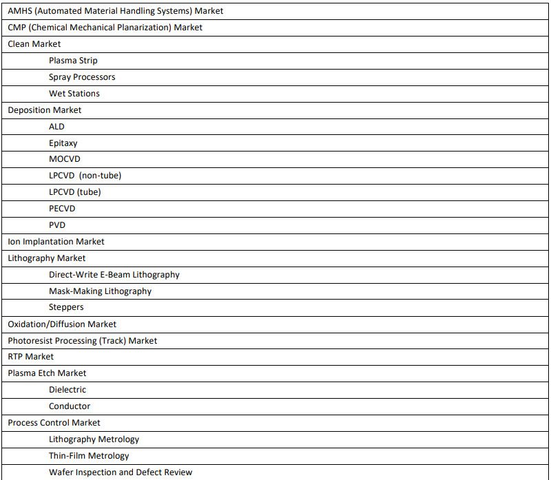
Chapter 3 Market Business Sectors Shares and Forecast 3-1
3.1 AMHS Market Shares and Forecast 3-1
3.2 CMP Market Shares and Forecast 3-4
3.3 Clean Market Shares and Forecast 3-7
3.3.1 Plasma Strip 3-8
3.3.2 Spray Processors 3-11
3.3.3 Wet Stations 3-14
3.4 Deposition Market Shares and Forecast 3-17
3.4.1 ALD 3-18
3.4.2 Epitaxy 3-21
3.4.3 MOCVD 3-24
3.4.4 LPCVD (non-tube) 3-27
3.4.5 LPCVD (tube) 3-30
3.4.6 PECVD 3-33
3.4.7 PVD 3-36
3.5 Ion Implantation Market Shares and Forecast 3-39
3.6 Lithography Market Shares and Forecast 3-42
3.6.1 Direct-Write E-Beam Lithography 3-43
3.6.2 Mask-Making Lithography 3-46
3.6.3 Steppers 3-49
3.7 Oxidation/Diffusion Market Shares and Forecast 3-52
3.8 Photoresist Processing (Track) Market Shares and Forecast 3-55
3.9 RTP Market Shares and Forecast 3-58
3.10 Plasma Etch Market Shares and Forecast 3-61
3.10.1 Dielectric 3-62
3.10.2 Conductor 3-65
3.11 Process Control Market Shares and Forecast 3-68
3.11.1 Lithography Metrology 3-69
3.11.2 Thin-Film Metrology 3-72
3.11.3 Wafer Inspection and Defect Review 3-75
Chapter 4 U.S. Semiconductor Equipment Suppliers - Profiles 4-1
4.1 Applied Materials 4-1
4.1.1 Business Sectors Covered In The Market Analysis Chapter 4-1
4.1.2 Company Profile 4-2
4.1.3 Company Financials 4-12
4.2 Axcelis Technologies 4-13
4.1.2 Business Sectors Covered In The Market Analysis Chapter 4-13
4.2.2 Company Profile 4-13
4.2.3 Company Financials 4-16
4.3 KLA 4-17
4.3.1 Business Sectors Covered In The Market Analysis Chapter 4-17
4.3.2 Company Profile 4-17
4.3.3 Company Financials 4-19
4.4 Lam Research 4-20
4.4.1 Business Sectors Covered In The Market Analysis Chapter 4-20
4.4.2 Company Profile 4-20
4.4.3 Company Financials 4-27
4.5 Mattson Technology 4-28
4.5.1 Business Sectors Covered In The Market Analysis Chapter 4-28
4.5.2 Company Profile 4-28
4.5.3 Company Financials 4-30
4.6 Opto Innovation 4-31
4.6.1 Business Sectors Covered In The Market Analysis Chapter 4-31
4.6.2 Company Profile - Nanometrics 4-31
4.6.3 Sectors Covered In The Market Analysis Chapter 4-35
4.6.4 Company Profile – Rudolph Technologies 4-35
4.6.5 Company Financials 4-38
4.7 Veeco 4-39
4.7.1 Business Sectors Covered In The Market Analysis Chapter 4-39
4.7.2 Company Profile 4-39
4.7.3 Company Financials 4-42
Chapter 5 European Semiconductor Equipment Suppliers - Profiles 5-1
5.1 Aixtron 5-1
5.1.1 Business Sectors Covered In The Market Analysis Chapter 5-1
5.1.2 Company Profile 5-1
5.1.3 Company Financials 5-3
5.2 ASM International 5-4
5.2.1 Business Sectors Covered In The Market Analysis Chapter 5-4
5.2.2 Company Profile 5-4
5.2.3 Company Financials 5-7
5.3 ASML 5-8
5.3.1 Business Sectors Covered In The Market Analysis Chapter 5-8
5.3.2 Company Profile 5-8
5.3.3 Company Financials 5-12
5.4 Carl Zeiss 5-13
5.4.1 Business Sectors Covered In The Market Analysis Chapter 5-13
5.4.2 Company Profile 5-13
5.4.3 Company Financials 5-15
5.5 Camtek 5-16
5.5.1 Business Sectors Covered In The Market Analysis Chapter 5-16
5.5.2 Company Profile 5-16
5.5.3 Company Financials 5-18
5.6 EV Group 5-19
5.6.1 Business Sectors Covered In The Market Analysis Chapter 5-19
5.6.2 Company Profile 5-19
5.6.3 Company Financials 5-21
5.7 LPE 5-22
5.7.1 Business Sectors Covered In The Market Analysis Chapter 5-22
5.7.2 Company Profile 5-22
5.7.3 Company Financials 5-22
5.8 Mycronic 5-23
5.8.1 Business Sectors Covered In The Market Analysis Chapter 5-23
5.8.2 Company Profile 5-23
5.8.3 Company Financials 5-24
5.9 Nova Measuring Instruments9 5-25
5.9.1 Business Sectors Covered In The Market Analysis Chapter 5-25
5.9.2 Company Profile 5-25
5.9.3 Company Financials 5-29
5.10 Oerlikon / Evatec 5-30
5.10.1 Business Sectors Covered In The Market Analysis Chapter 5-30
5.10.2 Company Profile 5-30
5.10.3 Company Financials 5-31
5.11 Semilab 5-32
5.11.1 Business Sectors Covered In The Market Analysis Chapter 5-32
5.11.2 Company Profile 5-32
5.11.3 Company Financials 5-33
Chapter 6 Asian Semiconductor Equipment Suppliers - Profiles 6-1
6.1 ACM Research 6-1
6.1.1 Business Sectors Covered In The Market Analysis Chapter 6-1
6.1.2 Company Profile 6-1
6.1.3 Company Financials 6-3
6.2 Advantest 6-4
6.2.1 Business Sectors Covered In The Market Analysis Chapter 6-4
6.2.2 Company Profile 6-4
6.2.3 Company Financials 6-5
6.3 AMEC 6-8
6.3.1 Business Sectors Covered In The Market Analysis Chapter 6-8
6.3.2 Company Profile 6-8
6.3.3 Company Financials 6-9
6.4 Avaco 6-10
6.4.1 Business Sectors Covered In The Market Analysis Chapter 6-10
6.4.2 Company Profile 6-10
6.4.3 Company Financials 6-11
6.5 Canon 6-12
6.5.1 Business Sectors Covered In The Market Analysis Chapter 6-12
6.5.2 Company Profile 6-12
6.5.3 Company Financials 6-14
6.5.6 Canon Anelva 6-16
6.6.1 Business Sectors Covered In The Market Analysis Chapter 6-16
6.6.2 Company Profile 6-16
6.6.3 Company Financials 6-17
6.7 Daifuku 6-18
6.7.1 Business Sectors Covered In The Market Analysis Chapter 6-18
6.7.2 Company Profile 6-18
6.7.3 Company Financials 6-19
6.8 Ebara 6-20
6.8.1 Business Sectors Covered In The Market Analysis Chapter 6-20
6.8.2 Company Profile 6-20
6.8.3 Company Financials 6-22
6.9 Eugene Technology 6-24
6.9.1 Business Sectors Covered In The Market Analysis Chapter 6-24
6.9.2 Company Profile 6-24
6.9.3 Company Financials 6-25
6.10 Hitachi High-Technologies 6-26
6.10.1 Business Sectors Covered In The Market Analysis Chapter 6-26
6.10.2 Company Profile 6-26
6.1.3 Company Financials 6-28
6.10 Hitachi Kokusai Electric 6-29
6.11.1 Business Sectors Covered In The Market Analysis Chapter 6-29
6.11.2 Company Profile 6-29
6.11.3 Company Financials 6-30
6.12 Hwatsing 6-31
6.12.1 Business Sectors Covered In The Market Analysis Chapter 6-31
6.12.2 Company Profile 6-31
6.12.3 Company Financials 6-31
6.13 JEOL 6-32
6.13.1 Business Sectors Covered In The Market Analysis Chapter 6-32
6.13.2 Company Profile 6-32
6.13.3 Company Financials 6-33
6.14 Jusung Engineering 6-33
6.14.1 Business Sectors Covered In The Market Analysis Chapter 6-34
6.14.2 Company Profile 6-34
6.14.3 Company Financials 6-35
6.15 KC Tech 6-36
6.15.1 Business Sectors Covered In The Market Analysis Chapter 6-36
6.15.2 Company Profile 6-36
6.15.3 Company Financials 6-37
6.16 Lasertec 6-38
6.16.1 Business Sectors Covered In The Market Analysis Chapter 6-38
6.16.2 Company Profile 6-38
6.16.3 Company Financials 6-39
6.17 Murata Machinery 6-40
6.17.1 Business Sectors Covered In The Market Analysis Chapter 6-40
6.17.2 Company Profile 6-40
6.17.3 Company Financials 6-41
6.18 Murata Machinery 6-42
6.18.1 Business Sectors Covered In The Market Analysis Chapter 6-42
6.18.2 Company Profile 6-42
6.18.3 Company Financials 6-44
6.19 Nikon 6-45
6.19.1 Business Sectors Covered In The Market Analysis Chapter 6-45
6.19.2 Company Profile 6-45
6.19.3 Company Financials 6-46
6.20 Nippon Sanso 6-48
6.20.1 Business Sectors Covered In The Market Analysis Chapter 6-48
6.20.2 Company Profile 6-48
6.20.3 Company Financials 6-49
6.21 Nissin Ion Equipment 6-50
6.21.1 Business Sectors Covered In The Market Analysis Chapter 6-50
6.21.2 Company Profile 6-50
6.21.3 Company Financials 6-50
6.22 NuFlare Technology 6-51
6.22.1 Business Sectors Covered In The Market Analysis Chapter 6-51
6.22.2 Company Profile 6-51
6.22.3 Company Financials 6-52
6.23 Piotech 6-53
6.23.1 Business Sectors Covered In The Market Analysis Chapter 6-53
6.23.2 Company Profile 6-53
6.23.3 Company Financials 6-53
6.24 PSK 6-54
6.24.1 Business Sectors Covered In The Market Analysis Chapter 6-54
6.24.2 Company Profile 6-54
6.24.3 Company Financials 6-55
6.25 Raintree Scientific Instruments 6-56
6.25.1 Business Sectors Covered In The Market Analysis Chapter 6-56
6.25.2 Company Profile 6-56
6.25.3 Company Financials 6-57
6.26 Screen Semiconductor Solutions 6-58
6.26.1 Business Sectors Covered In The Market Analysis Chapter 6-58
6.26.2 Company Profile 6-58
6.26.3 Company Financials 6-60
6.27 SEMES 6-61
6.27.1 Business Sectors Covered In The Market Analysis Chapter 6-61
6.27.2 Company Profile 6-61
6.27.3 Company Financials 6-62
6.28 SEN 6-63
6.28.1 Business Sectors Covered In The Market Analysis Chapter 6-63
6.28.2 Company Profile 6-63
6.28.3 Company Financials 6-63
6.29 TES 6-64
6.29.1 Business Sectors Covered In The Market Analysis Chapter 6-64
6.29.2 Company Profile 6-64
6.29.3 Company Financials 6-65
6.30 Tokyo Electron 6-66
6.30.1 Business Sectors Covered In The Market Analysis Chapter 6-66
6.30.2 Company Profile 6-66
6.30.3 Company Financials 6-69
6.31 Tokyo Seimitsu 6-70
6.31.1 Business Sectors Covered In The Market Analysis Chapter 6-70
6.31.2 Company Profile 6-70
6.31.3 Company Financials 6-71
6.32 Topcon Technohouse 6-72
6.32.1 Business Sectors Covered In The Market Analysis Chapter 6-72
6.32.2 Company Profile 6-72
6.32.3 Company Financials 6-72
6.33 Toray Engineering 6-73
6.33.1 Business Sectors Covered In The Market Analysis Chapter 6-73
6.33.2 Company Profile 6-73
6.33.3 Company Financials 6-74
6.34 Ulvac 6-75
6.34.1 Business Sectors Covered In The Market Analysis Chapter 6-75
6.34.2 Company Profile 6-75
6.34.3 Company Financials 6-76
6.35 Ushio 6-77
6.35.1 Business Sectors Covered In The Market Analysis Chapter 6-77
6.35.2 Company Profile 6-77
6.35.3 Company Financials 6-77
6.36 Wonik IPS 6-78
6.36.1 Business Sectors Covered In The Market Analysis Chapter 6-78
6.36.2 Company Profile 6-78
6.36.3 Company Financials 6-78
List of Tables/GraphsLIST OF TABLES
1.1 Global Wafer Front End Equipment Companies 1-2
1.2 Capex By Company 1-5
2.1 Foundry Capex ($ Millions) 2-3
2.2 Pure Play Foundry Forecast 2-5
2.3 Pure Play Foundry Revenue Shares 2-7
2.4 Foundry / Logic Lithography Demand 2-9
2.5 New Capacity Equipment Demand By Type 2-10
2.6 TSMC Wafer Price By Node – 1995-2025 2-11
2.7 TSMC Wafer Price By Node – 2025 2-12
2.8 TSMC Chip Features By Node 2-13
2.9 TSMC Top Customers By Revenue 2-14
2.10 Technology Roadmaps For China Foundries 2-16
2.11 Global Foundry Market By Linewidth 2-17
2.12 Foundry Capacity By Region 2-19
2.13 DRAM Wafer Capacity Forecast by Fab - Wafers 2-21
2.14 DRAM Earnings Comparisons by Company 2-22
2.15 DRAM Revenue Demand Forecast by Application 2-23
2.16 DRAM Market Shares 2-25
2.17 DRAM Capex Forecast by Company 2-26
2.18 NAND Wafer Capacity by Fab 2-28
2.19 NAND Earnings Comparison by Company 2-29
2.20 NAND Bit Growth Demand Forecast by Application 2-30
2.21 NAND Market Shares 2-32
2.22 Average Selling Prices (ASPs) Forecast 2-33
2.23 NAND Capex Forecast By Company 2-34
2.24 China Manufacturing Capacity 2-38
2.25 Chinese Equipment Suppliers And Top Foreign Supplier 2-39
2-26 China’s 8- And 12-Inch Fabs and Foundries 2-49
3.1 AMHS Market Forecast 3-2
3.2 CMP Market Forecast 3-5
3.3 Plasma Strip Market Forecast 3-9
3.4 Spray Processors Market Forecast 3-12
3.5 Wet Stations Market Forecast 3-15
3.6 ALD Market Forecast 3-19
3.7 Epitaxy Market Forecast 3-22
3.8 MOCVD Market Forecast 3-25
3.9 LPCVD (non-tube) Market Forecast 3-28
3.10 LPCVD (tube) Market Forecast 3-31
3.11 PECVD Market Forecast 3-34
3.12 PVD Market Forecast 3-37
3.13 Ion Implantation Market Forecast 3-40
3.14 Direct-Write E-Beam Lithography Market Forecast 3-44
3.15 Mask-Making Lithography Market Forecast 3-47
3.16 Steppers Market Forecast 3-50
3.17 Oxidation Market Forecast 3-53
3.18 Photoresist Processing (Track) Market Forecast 3-56
3.19 RTP Market Forecast 3-59
3.20 Dielectric Etch Market Forecast 3-63
3.21 Conductive Etch Market Forecast 3-66
3.22 Lithography Metrology Market Forecast 3-70
3.23 Thin-Film Metrology Market Forecast 3-73
3.24 Wafer Inspection and Defect Review Market Forecast 3-76
LIST OF FIGURES
1.1 Semiconductor Equipment Billings 1-6
2.1 China’s IC Production Forecast 2-40
2.2 China’s IC Consumption 2-42
2.3 China’s IC Production/Consumption Ratio 2-43
2.4 IC Import to China 2-44
2.5 China’s IC Supply/Demand 2-45
2.6 China’s IC Fab Capacity 2-47
2.7 China’s IC Fab Capacity by Region 2-48
2.8 China’s IC Fab Capacity by Wafer Size 2-51
2.9 China’s IC Fab Capacity by Geometry 2-52
2.10 China’s IC Production by Application 2-54
3.1 AMHS Market Shares 3-3
3.2 CMP Market Shares 3-6
3.3 Plasma Strip Market Shares 3-10
3.4 Spray Processors Market Shares 3-13
3.5 Wet Stations Market Shares 3-16
3.6 ALD Market Shares 3-20
3.7 Epitaxy Market Shares 3-23
3.8 MOCVD Market Shares 3-26
3.9 LPCVD (non-tube) Market Shares 3-29
3.10 LPCVD (tube) Market Shares 3-32
3.11 PECVD Market Shares 3-35
3.12 PVD Market Shares 3-38
3.13 Ion Implantation Market Shares 3-41
3.14 Direct-Write E-Beam Lithography Market Shares 3-45
3.15 Mask-Making Lithography Market Shares 3-48
3.16 Steppers Market Shares 3-51
3.17 Oxidation Market Shares 3-54
3.18 Photoresist Processing (Track) Market Shares 3-57
3.19 RTP Market Shares 3-60
3.20 Dielectric Etch Market Shares 3-64
3.21 Conductive Etch Market Shares 3-67
3.22 Lithography Metrology Market Shares 3-71
3.23 Thin-Film Metrology Market Shares 3-74
3.24 Wafer Inspection and Defect Review Market Shares 3-77
ご注文は、お電話またはWEBから承ります。お見積もりの作成もお気軽にご相談ください。本レポートと同分野(半導体)の最新刊レポート
The Information Network社の スペシャルレポート分野 での最新刊レポート関連レポート(キーワード「半導体製造装置」)
よくあるご質問The Information Network社はどのような調査会社ですか?インフォメーションネットワーク (The Information Network) は、半導体製造に関連する材料や半導体のエンドアプリケーションなどの市場を幅広く調査・分析する米国ペンシルベニア州の調... もっと見る 調査レポートの納品までの日数はどの程度ですか?在庫のあるものは速納となりますが、平均的には 3-4日と見て下さい。
注文の手続きはどのようになっていますか?1)お客様からの御問い合わせをいただきます。
お支払方法の方法はどのようになっていますか?納品と同時にデータリソース社よりお客様へ請求書(必要に応じて納品書も)を発送いたします。
データリソース社はどのような会社ですか?当社は、世界各国の主要調査会社・レポート出版社と提携し、世界各国の市場調査レポートや技術動向レポートなどを日本国内の企業・公官庁及び教育研究機関に提供しております。
|
|